Low Output Voltage Synchronous Boost Regulators Extend Battery Life in Single Cell Applications
Low Output Voltage Synchronous Boost Regulators Extend Battery Life in Single Cell Applications
著者
Mark Jordan
2002年03月01日
Introduction
The LTC3423 and LTC3424 Synchronous Boost Regulators are designed for single cell (Alkaline, NiMH, or NiCd) portable electronics that require a low voltage supply, typically between 1.5V to 2.5V, at load currents up to 0.8 amps. These products are designed to prolong battery life for applications where an available higher voltage supply (2.7V to 5.5V) can provide internal bias for the IC. Before the LTC3423 and LTC3424 became available, power supplies for low voltage, high current solutions included a buck converter from the higher voltage output, a simple, but relatively inefficient solution. These new devices offer a solution that is just as simple, but with much improved efficiency. The simple block diagrams in Figures 1A and 1B show how this difference arises: double conversion is shown Figure 1A, and the approach of regulating the low voltage supply directly from the cell is shown in Figure 1B.

Figure 1a. Commonly used, but inefficient boost-buck solution for generating a 1.8V high current output

Figure 1b. A more efficient solution boosts directly from the battery to get the 1.8V output
Features
Both devices are additions to the family of 3MHz, Micropower Synchronous Boost Regulators, intended for low output voltage applications. High frequency operation allows the use of a small surface mount inductor and tiny ceramic capacitors. Efficiencies of up to 95% are achieved through internal features such as loss less current sensing, low gate charge-low RDS(ON) synchronous power switches and fast switching transitions to minimize power loss. An external Schottky diode is not required, but can be added to maximize efficiency. An applied bias voltage of at least 2.7V is required for the internal gate drive and supply of the IC.
The LTC3423 is optimized for applications requiring 0.6 watts or less of output power, whereas the LTC3424 is optimized for applications requiring 1.2 watts or less. Both converters offer programmable operating frequencies from 100kHz to 3MHz via a resistor from the RT pin to ground. Output voltage is adjustable from 1.5V to 5.5V with a simple resistor voltage divider to the FB (feedback) pin. The transient response can be optimized over a wide range of loads and output capacitors via current mode control architecture, OPTI-LOOP® compensation and adaptive slope compensation.
To further improve efficiency for light loads, the user can take advantage of high efficiency Burst Mode, where the IC consumes only 38µA of quiescent current. Burst Mode operation is enabled by driving the MODE/SYNC pin high, otherwise fixed frequency switching is enabled when driving the MODE/SYNC pin low. The operating frequency can be set externally by connecting a clock to the MODE/SYNC pin. The part can also be shut down, drawing less than 1µA of quiescent current.
Single Cell to 1.8V at 700mA Application
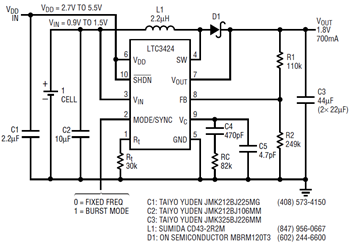
Figure 2 shows a circuit for generating 1.8V directly from the single cell at 700ma load current. Figure 3 shows the efficiency curves over the operating voltage range of the battery. The efficiency peaks at 95% with a fresh battery, and drops to 90% when the battery terminal voltage is 0.9V. If Burst Mode is enabled at light loads, the efficiency stays above 70% down to a 500µA load.

Figure 2. Application for a single cell to 1.8V at 700mA using the LTC3424

Figure 3. Efficiency curve for the circuit in Figure 2 at various battery input voltages
Conclusion
Linear Technology’s Low Output Voltage Synchronous Boost converters allow designers of handheld electronics to efficiently regulate a voltage as low as 1.5V directly from a single cell. They provide solutions for prolonged battery life, small circuit board size and easy programmability all in a small MSOP-10 Package.


