High Linearity, Low Noise LTC2387-18 Drivers for Sinusoidal Signals
Introduction
The LTC2387-18 is a high speed SAR (Successive Approximation Register) ADC suited for high linearity, low noise applications. This ADC is capable of sampling at up to 15Msps, which allows it to convert signals at frequencies of several MHz. It is well-suited to convert both pulsed and continuous signals in this frequency range. This article will address the need for drivers designed to deliver continuous sinusoidal signals to the ADC. The noise performance is such that a 1MHz tone will yield an SNR of over 96dBFS. The total harmonic distortion of this tone will typically exceed -100dB. To drive the ADC to full scale requires a differential input signal of 8.192V pk-pk.
Many sensor and signal sources do not deliver this much voltage swing, or are not able to drive the relatively low input impedance of the ADC. Buffer circuits are best suited to solve these problems, but they must be very linear and contribute little noise to the signal. Often the buffer circuit must present an impedance to the source that does not load it unduly, and provide voltage gain. Op amps, whether single-ended or differential, must be very high performance if the overall circuit is to approach the specifications met by the ADC.
Buffer Circuit Overview
If a differential input signal is available, the buffer circuit will perform three functions. First, a small amount of input lowpass filtering is used to limit the noise spectrum reaching the amplifiers. The signal is then buffered, usually with one op amp per side. In some cases, the buffers include some voltage gain. This eases the drive requirement from the signal source, but can degrade SNR as this gain amplifies the noise from the source. Lastly, the signal is lowpass filtered again before it is passed on to the ADC. This function is served by an RC filter that further limits the broadband noise reaching the ADC input. The filter also provides some series resistance before the filter capacitor, which presents the amplifier with a less reactive load impedance. The capacitance serves as a charge reservoir for the sampling transients from the ADC input circuit. This reduces the size of the sampling charge pulses at the amplifier output. If the capacitance is too large, however, the overall network will not settle completely enough between sampling instants. In some cases a differential input signal is not available. The buffer circuit must then perform the additional function of deriving a differential signal from a single-ended one.
Basic Buffer Circuit
A basic buffer circuit for driving the LTC2387-18 is shown in Figure 1 below.
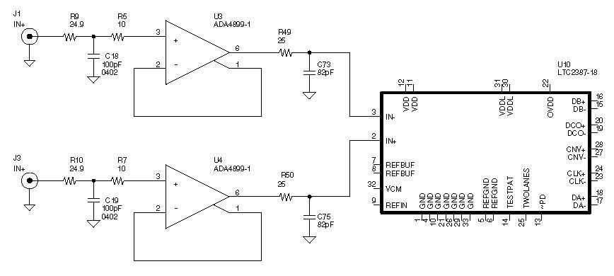
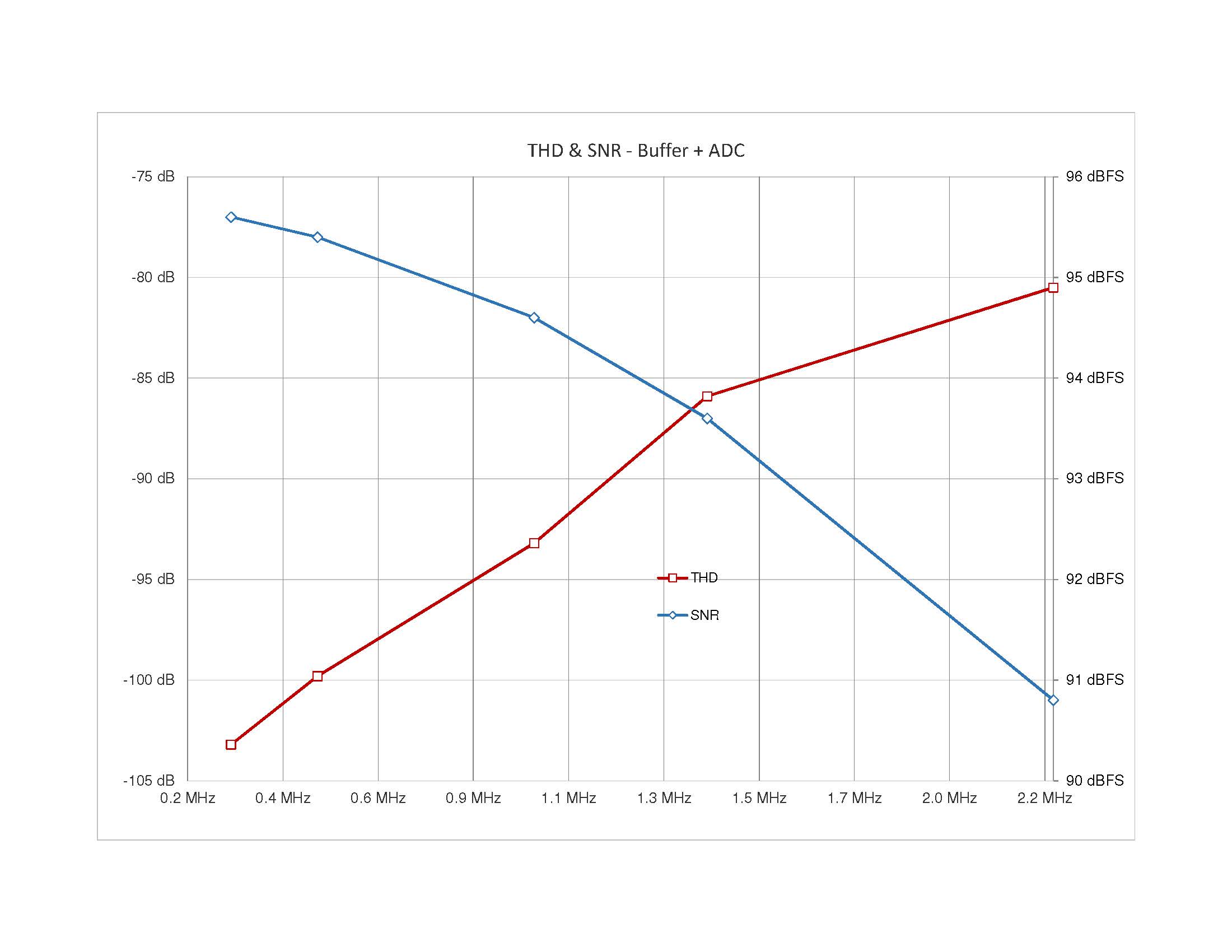
The amplifiers operate from +7.5V/-2.5V supply rails. The input circuit provides a lowpass pole near 31MHz, assuming a 25Ω source impedance. Larger values of source impedance will lower this pole frequency. The series resistance also satisfies the required 25Ω at the input of the ADA4899-1 in unity gain configuration. At each amplifier output is a 25Ω series resistor. The lowpass section formed by these resistors, along with the 82pF capacitors, yields a pole near 77MHz. These capacitors are as large as possible, without degrading the settling time of the network. This circuit is very simple, and presents a high load impedance to customer signal sources. It does not provide voltage gain, however. It also accommodates DC-coupled signals only; the DC level of the input signals must be close to 2.048V. Performance data for this circuit over the range of 300KHz to 2.2MHz appears in Figure 2 below.
Single-Ended Input Signal Buffer Circuit
If a differential input signal is not available, the buffer circuit can be modified to accept a single-ended one. The schematic shown in Figure 3 is an example of this.
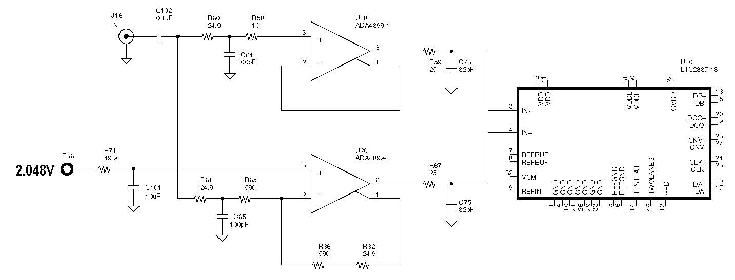
The circuit uses a precision reference applied at Vcm to establish the common-mode voltage of both outputs. This allows the use of an AC coupled input, but creates an avenue for noise ingress. In a unity gain configuration, such as shown in Figure 3, any noise or spurious signals at the reference voltage port appear as differential disturbances at the outputs on a one-to-one gain basis. The voltage reference chosen for this port must be as quiet as possible, and heavily filtered before it is applied to the non-inverting terminal of the op amp. The series and feedback resistors around the inverting amplifier also contribute broadband noise to the output. Minimizing the magnitude of these resistors is critical to reducing this contribution. Even with careful design the effects of the reference and resistors are sizeable, and the SNR of this configuration is several dB below that of the true differential buffer circuit. Performance data for the single-ended buffer circuit appears in Figure 4.

Buffer with Absorptive Filter Circuit
The filter used at the output of the simple buffer circuits consists of only a series resistor and a shunt capacitor. The selectivity of such a filter is poor, and the impedance presented to the amplifiers is low near the corner frequency. The input impedance of the filter section is very high, and changes rapidly with frequency within the passband. This type of filter rejects out-of-band signals through reflection, rather than absorption. A filter with more poles and absorptive elements can provide a more well-behaved load impedance as well as more out-of-band rejection. An example of this type of filter is shown in Figure 5.
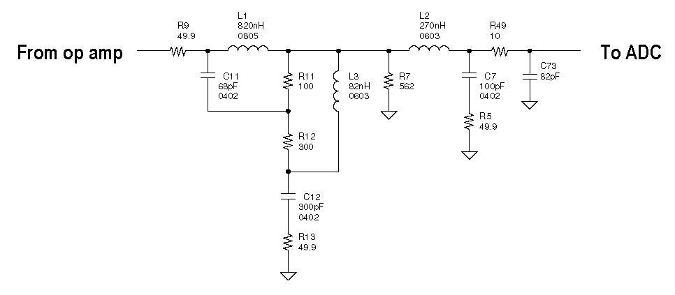
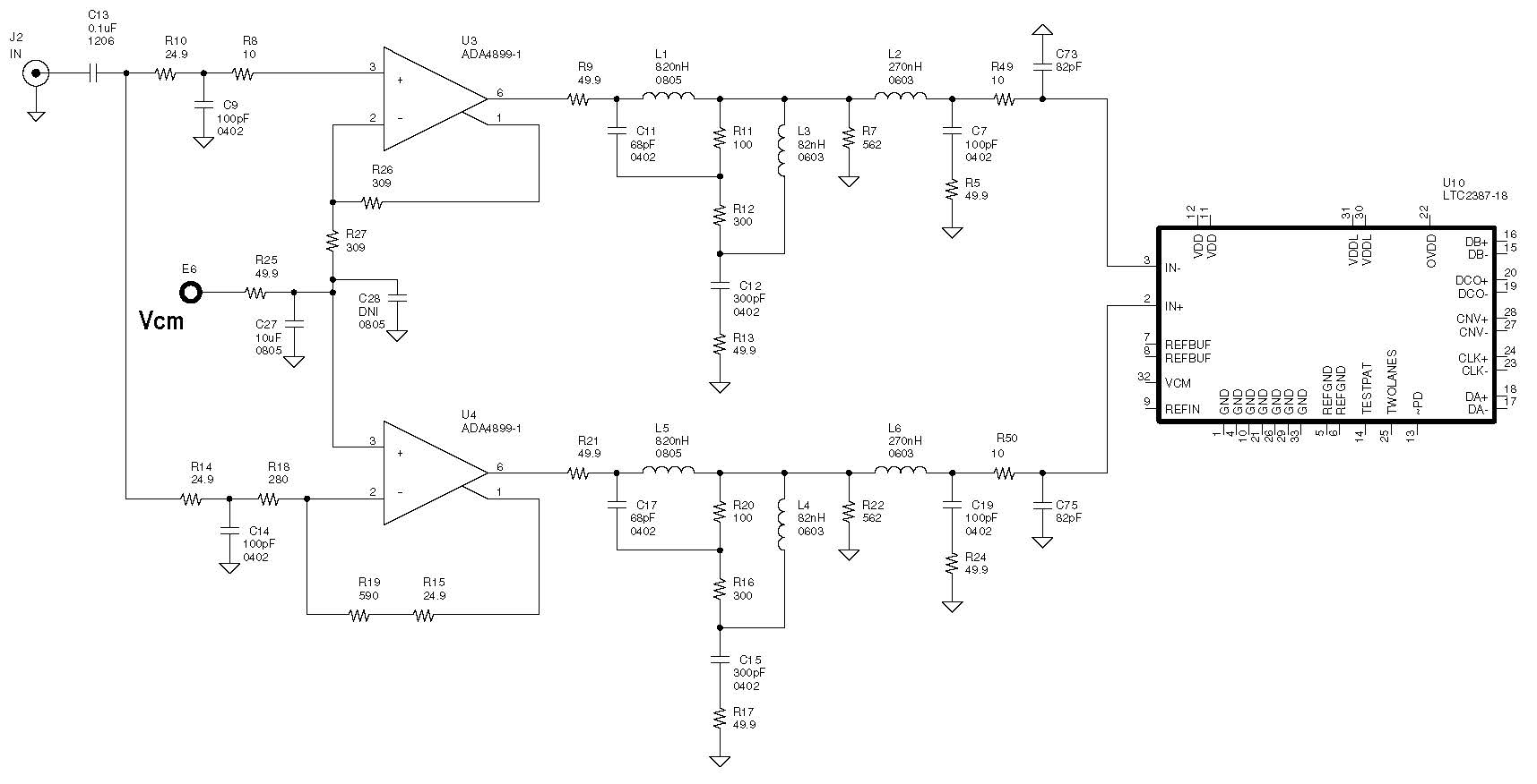
This filter presents a load impedance of 300Ω within much of the passband, dropping to 150Ω at 1MHz. The 3dB corner is near 9MHz, providing a much narrower passband than the simple RC filter. The absorptive driver board uses a differential version of the filter in figure 5 to provide much better SNR. A simplified schematic appears in Figure 6 below.
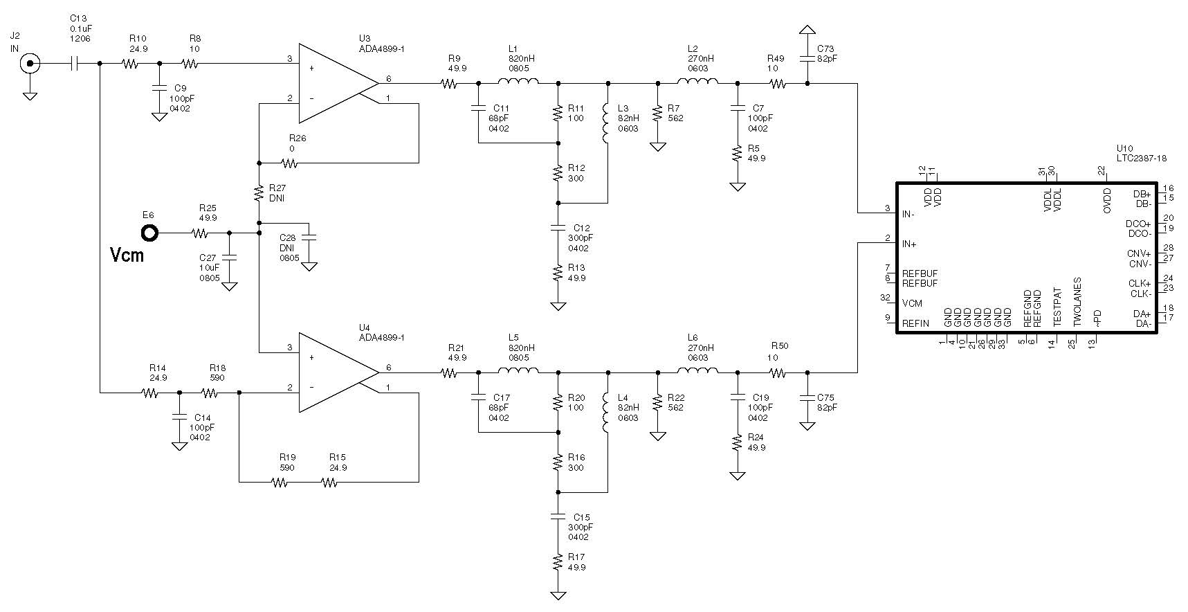
This circuit can easily be configured to provide voltage gain; Figure 7 shows an example with a voltage gain of 4.
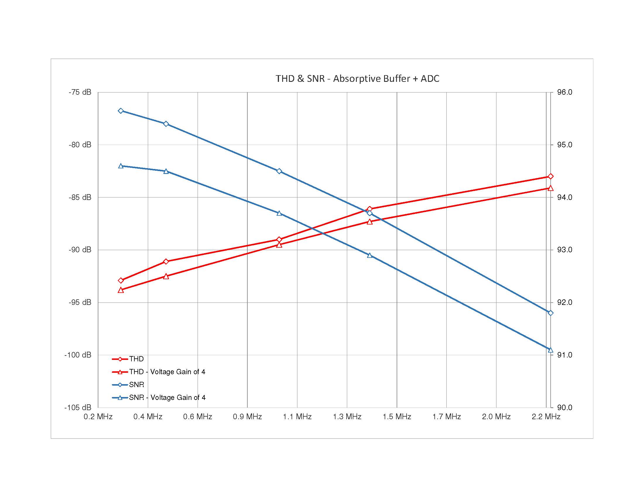
Performance data for both circuits appears in Figure 8 below.
Feedback Amplifier + Absorptive Filter
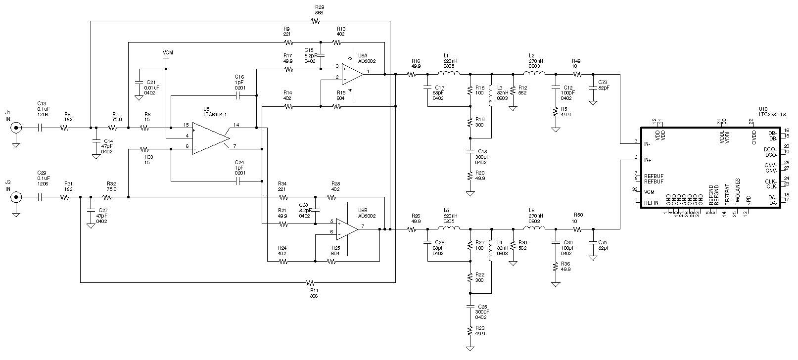
The circuits presented thus far are very straightforward, using op amps followed by lowpass filters. A more sophisticated approach has also been evaluated, which employs local and global feedback to improve the linearity of the amplifiers. The primary amplifier is an LTC6404, which is a low noise, low distortion differential amplifier. Following this amplifier are two AD8002 current feedback op amps. These op amps serve two purposes. First, they provide a voltage gain of 4, which converts the 2V peak-to-peak output voltage swing of the LTC6404 to the 8V peak-to-peak swing required to drive the ADC to full scale. Also, these op amps are current feedback devices, which means they offer higher slew rate and lower output impedance. Both of these attributes are well-suited to drive the ADC inputs via the previously described absorptive lowpass filters. This circuitry is derived partially from the ADC driver circuit described in “How to Drive the LTC2387 (Part 1): Signal Applications to 5MHz That Require Low Intermodulation Distortion”, Linear Technology Blog, by Derek Redmayne. A simplified schematic appears in Figure 9.
Performance data for this circuit appears in Figure 10 below.

The circuits and data presented herein show there are cases where improved SNR may be traded for circuit complexity or distortion, for example. Note that the data presented herein was taken using a single DC2290A demo board, driven by separate demo boards for the buffer circuits.
Several of these circuits are available as demo boards from LTC:
Simple Buffer Circuit: - contact author
Single-ended to Differential Buffer Circuit: - contact author
Buffer with Absorptive Filter Circuit: - DC2622A
Feedback Amplifier with Absorptive Filter Circuit: - DC2623A
LTC2387-18 Demo Board: - DC2290A


