
未来のイノベーションを支える中間バス・コンバータ【Part 3】2kWの出力に対応するクォータ・ブリック電源のリファレンス設計
シリーズの関連記事を読む
主なポイント
|
概要
現在は、AI、機械学習、クラウド・ベースのアプリケーションに対する依存度が急速に増大している状況にあります。それに伴い、小型かつ高効率で信頼性に優れる電力変換ソリューションに対する需要がかつてないほど高まっています。既存のデータ・センターでは、48Vの入力電圧を降圧する中間バス・コンバータが使用されてきました。なかでも一般的なものだと言えるのがクォータ・ブリック(QB:Quarter Brick)電源です。本稿では、このクォータ・ブリック電源のリファレンス設計を紹介します。その回路は、アナログ・デバイセズのディスクリート型ソリューションを活用することにより、CFP(Common Footprint Package)に即したサイズで設計されています。それだけでなく、市販の製品に勝る性能を発揮します。このリファレンス設計は、高性能のアプリケーションに最適な競争力と拡張性に優れるソリューションです。ハイパースケール・コンピューティングや産業用システムなどで求められる厳しい要件を満たしています。
はじめに
本稿で紹介するのは、クォータ・ブリック・モジュール(以下、QBM)のリファレンス設計です。この高性能のDC/DCコンバータは、アナログ・デバイセズのクォータ・ブリック・システム向けのアーキテクチャをベースとしています。この設計では、新たな結合インダクタ(CL:Coupled Inductor)を採用しています。また、DOSA(Distributed-Power Open Standards Alliance)の厳しい寸法の要件を満たしつつ、CFPに即したサイズで2kWの電力を連続して供給できるようになっています。このような設計手法により、ハード・スイッチング・コンバータで生じる電力損失を低減し、動作効率の高いQBMを構築することができました。その結果、要件が非常に厳しいアプリケーションに対応可能な堅牢性の高いソリューションが完成しました。
このリファレンス設計では、48V/54Vから12Vへの降圧を担うアナログ・デバイセズの新たな中間バス変換(IBC:Intermediate Bus Conversion)技術を活用しています。それにより複雑さが軽減されるので、お客様は開発期間を短縮できます。本稿で示す包括的なデータは、この設計によって効率、熱性能、スケーラビリティが大きく改善することを実証するものです。つまり、このソリューションは、より多くの電力を消費するデータ・センターに最適な次世代のQBMだと言えます。そのアーキテクチャは、現在のIBCに求められる要件に対応するだけでなく、400V~800Vの入力電圧を使用する将来の電源システムへの道筋を示すものでもあります。
QBMの設計
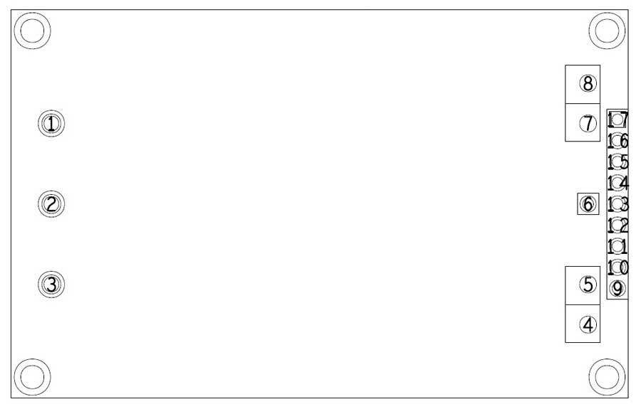
本稿で紹介するQBMのリファレンス設計(以下、これをQBMと表記することにします)では、DOSAの規格に即した一般的な機械的ピン配置を採用しています(図1)。そのため、システムで使用している既存のボードにシームレスに統合できます。このQBMを単一のモジュールとして動作させる場合、管理用のインターフェースとして必要になるのはPMBus®の信号だけです。表1に、QBMの各ピンの概要をまとめました。
| ピン番号 | ピン名 | 機能 |
| 1 | +VIN | 正の入力ピン |
| 2 | RC | DC/DCのイネーブル |
| 3 | -VIN | 負の入力ピン |
| 4.5 | -VO | 負の出力ピン |
| 6 | PG | パワー・グッド |
| 7, 8 | +VO | 正の出力ピン |
| 9 | SS | ソ フト・ス タ ート・ピ ン |
| 10 | CLK_IN | 外部クロック入力 |
| 11 | -VSNS | 負のリモート・センス出力 |
| 12 | SDA | PMBusのデータ |
| 13 | SALERT | PMBusのアラート |
| 14 | SCL | PMBusのクロック |
| 15 | SA1 | PMBusのASEL1(アドレス設定、トライステート) |
| 16 | SA0/+VSNS | PMBusのASEL0(アドレス設定、トライステート)/ 正のリモート・センス出力 |
| 17 | ISHARE | アクティブ電流の共有ピン |
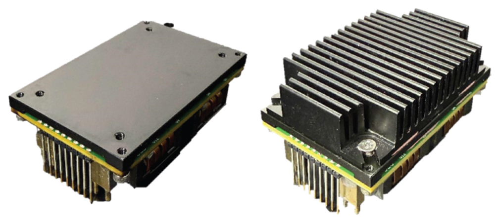
このQBMは、上部が平坦なベースプレートを備えています(図2)。その役割は、DC/DCコンバータのFET(パワー・スイッチ)を効果的に冷却することです。このベースプレートは、温度を最適に管理できるように設計されています。QB電源向けの市販のヒート・シンクと組み合わせることで、より多くの出力電力に対応できるようになります。
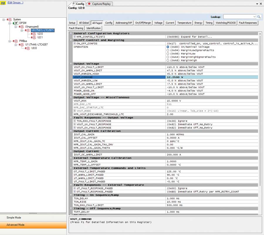
アナログ・デバイセズは、パワー・マネージメントIC用の開発環境「LTpowerPlay®」を提供しています。このソフトウェアとドングル「DC1613」を併用すれば、QBMを容易に構成(コンフィギュレーション)することができます。まず、一般的な動作パラメータの設定が行えます。また、障害に対応するトリガのレベルとそれに対応する応答を定義することが可能です。更に、包括的な監視/制御に向けて、動作に関するログを記録するための設定を実施できます。図3に、LTpowerPlayのGUIを使用してQBMの構成を行っている様子を示しました。
電気的な性能
ここからは、QBMの主要な電気的性能の評価結果を示すことで、その設計の優位性を明らかにしていきます。QBMにおいて特に重要なパラメータは、効率とそれに関連する電力損失です。正確な評価を実施するために、効率の測定は端子の手前で行うことにしました。その目的は、DC/DCコンバータの部分だけの性能を評価できるようにすることです。なお、システム全体を最適化するために、カスタムの端子を設計して使用しても構いません。図4に示したのが効率の評価結果です。入力電圧を48V~60Vの範囲で変化させて測定を行いました。
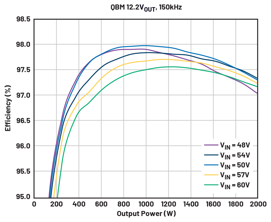
ご覧のとおり、このQBMは、全負荷時に97%以上、ピーク時に98%近くに達する卓越した効率を達成しています。このような性能を備えているということは、電力損失が非常に少なく抑えられているということを意味します。そのため、温度の管理が容易になります。結果として、データ・センターにおける冷却の要件を緩和することが可能になります。また、このQBMは入力電圧が50Vの場合に向けて最適化されています。つまり、800Vの電源電圧を使用し、16:1で降圧された電圧がQBMに入力されるケースを想定しています。将来のデータ・センターでは、そうした高電圧に対応するアーキテクチャが使用されるようになるでしょう。このQBMは、それを見据えた理想的な降圧コンバータだと言えます。
熱性能
熱性能は、電力密度の高いソリューションにおける重要な指標です。技術的には大電力の出力に対応可能なDC/DCコンバータであっても、その能力は最終的に実装先となる空間内の熱設計によって制限されます。本稿で取り上げているQBMについては、限られたスペースで動作させる場合でも、過熱によってシャットダウン機能がトリガされることなく、定格の出力電力を供給できることが実証されています。
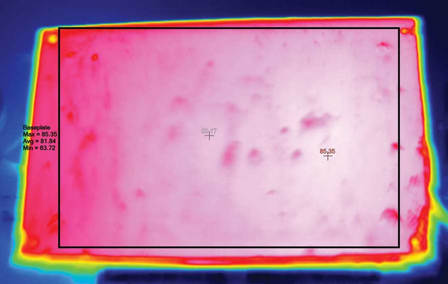
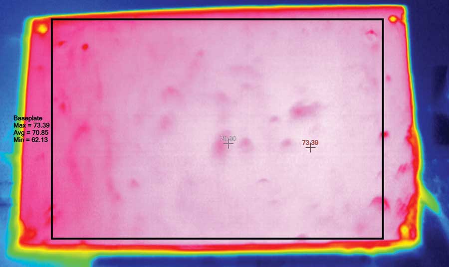
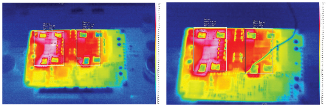
図5、図6に示したのは、それぞれ入力電圧が48V、54Vである場合のQBMの熱画像です。これらの結果を見ると、ベースプレート(ヒート・シンクなし)の表面全体に温度が均一に分布しています。つまり、ホットスポットからの偏差が最小限に抑えられているということです。この結果は、重要なコンポーネントを適切に配置し、銅箔レイヤのレイアウトを効果的に設計したことによって得られています。そのようにすることで、熱の集中を最小限に抑えられました。言い換えれば、熱的な制約のない信頼性の高い動作が確保されるということです。
障害が発生した場合の応答
このQBMは、パワー・マネージメント用のコントローラICとして「LTC2971」を採用しています。そのため、PMBus Level 1に対応していることになります。同ICは、電圧、電流、温度といった主要なパラメータを監視します。そして、障害が発生した場合には適切に対処するための機能を起動します。特定の障害については、より有用な設定が行えるようになっています。すなわち、QBMをラッチされた状態で維持するか、再試行するかという選択が可能です。このような機能により、高い柔軟性と堅牢性でシステムを保護します。
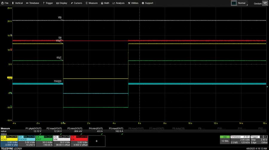
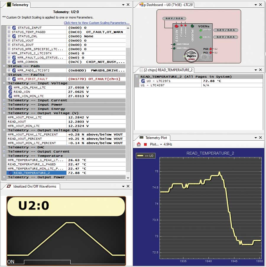
図7に示したのは、過熱保護(OTP:Overtemperature Protection)のテストを実施した結果です。このテストでは、温度が75℃に達するとQBMがシャットダウンするように設定しました。また、トリップ後の回復時間は5秒に設定しています。
図8に示したのは、LTpowerPlayによるOTPの検証結果です。図中のグラフも、QBMの温度が75℃に達するとシャットダウンすることを表しています。この設定は、LTpowerPlayのGUIによって行えます。なお、実際のQBMでは、OTPの機能が働く温度は90℃に設定されています。
並列動作
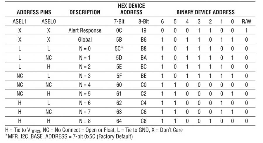
本稿で紹介しているQBMには、もう1つ重要な特徴があります。それは、より多くの供給電力が求められる場合に対応するために、複数のQBMを並列に動作させられるようになっているというものです。具体的には、最大9台のQBMを並列動作させることができます。また、その数は、図9に示すLTC2971のアドレス設定によって指定できます。
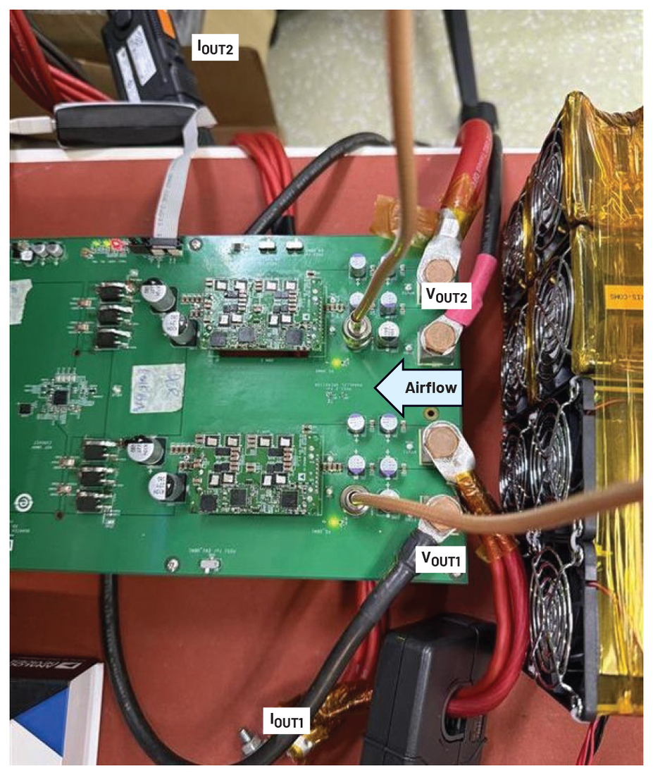
続いて、並列動作の評価結果を示します。図10において、エアフローは右側から左側に向かって流れています。この環境を使用し、QBM内部の出力段に対応するホットスポットについて評価しました。なお、この環境では、ベースプレートを使用しない状態で評価を実施することも可能です。
並列動作の性能は、各QBM間の電流量にどれだけの差があるのかを計測することによって評価できます。図11に示したのは、2つのQBMを使用し、計4kWの電力を出力している場合の測定結果です。電流量の差が小さいほど、電流の分担を良好に実現できていることになります。このことは、各QBMが同じ熱条件の下で確実に動作するようにし、全QBMの出力能力を最大化する上で重要な意味を持ちます。図12に、この評価によって得られた結果をまとめました。両出力電流にどの程度の差があるのかを確認できます。
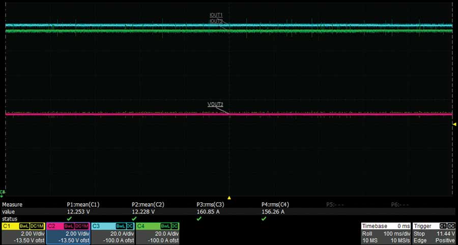
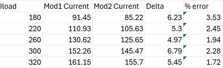
図13に示したのは、2つのQBMによって4kWの電力を出力した場合の熱画像です。これらはベースプレートを使用しない状態で取得しました。ご覧のように、両QBMのボードの熱性能は同様のプロファイルを示していることがわかります。各部の温度差は10℃未満に抑えられています。
ここまで、QBMの主要な性能の評価結果を示してきました。それらを見れば、アナログ・デバイセズのQBMは、CFPに即したIBCのアプリケーションにおいて最高レベルの性能を発揮し、大電力を供給できることがわかります。つまり、堅牢性と競争力に優れるシンプルなソリューションだと言えます。
まとめ
既存のデータ・センターは、大きな課題に直面しています。AIや機械学習の急速な進歩に牽引され、コンピューティング・システムにはより高い性能が求められるようになりました。それに伴い、システムの消費電力も急増しています。データ・センターは、そのような電力需要の増大に対応しなければなりません。データ・センターの既存のアーキテクチャでは、より電力密度の高いソリューションが使われています。すなわち、48V/54Vのバス電圧を使用することで、12Vを使用する旧来のシステムと比べて電力損失が大幅に削減されています。この移行において重要な役割を果たすのがIBCです。なかでも、コンパクトで高効率のクォータ・ブリック電源は特に重要な存在だと言えます。同電源は、高電圧のDC入力を基に、プロセッサやペリフェラル・システムに必要な低い電源電圧を生成します。
AIに関連するアプリケーションは急速に進化しています。そうしたなか、48V/54Vに対応するアーキテクチャによって、増大する電力需要に対応し続けることは可能なのでしょうか。本稿では、この重要な問いに答えるべく設計されたアナログ・デバイセズの最新のソリューションを紹介しました。
参考資料
Sam Ben-Yaakov、Michael Evzelman「Generic and Unified Model of Switched Capacitor Converters(スイッチド・キャパシタ・コンバータの汎用/統一モデル)」2009 IEEE Energy Conversion Congress and Exposition、2009年
Christian Cruz「48Vの電源電圧がシステム・レベルのアプリケーションにもたらすメリット」Analog Dialogue、Vol. 58、2024年7月
Michael Evzelman、Shmuel Ben-Yaakov「Average-Current -Based Conduction Losses Model of Switched Capacitor Converters(スイッチド・キャパシタ・コンバータにおける平均電流ベースの伝導損失のモデル)」IEEE Transactions on Power Electronics、Vol. 28、No. 7、2012年10月
Alexandr Ikriannikov、Laszlo Lipcsei「結合インダクタを活用した多相降圧レギュレータ、48Vから12Vへの変換効率が大幅に向上」Analog Devices、Vol. 58、2023年10月
Samuel Webb、Yan-Fei Liu「A Novel Intermediate Bus Converter Topology for Cutting Edge Data Center Applications(最先端のデータ・センター・アプリケーションに適した新たな中間バス・コンバータのトポロジ)」Chinese Journal of Electrical Engineering、Vol. 6、No. 4、2020年12月
「結合インダクタ技術の利点」Analog Devices、2015年