The Missing Middle in AESA Development: From Beamforming ICs to Scalable Apertures

The Missing Middle in AESA Development: From Beamforming ICs to Scalable Apertures
著者
Jeff Massman
2026年10月14日
Key Takeaways
|
Abstract
Multichannel beamforming ICs and integrated front ends have lowered the barrier to assembling phased array RF channels. However, conducted component evidence does not establish their behavior after connection to an antenna lattice. At the phased array tile boundary, embedded-element behavior, calibration, timing, heat flow, mechanics, and over-the-air validation become coupled. This article examines that missing middle through a modular X-band aperture platform. Its 16-element active tile and measured four-tile, 64-element assembly demonstrate a common building-block architecture that preserves reusable interfaces while aperture size, power, cooling, channel partitioning, and back-end processing change with the mission. The tile antenna covers 8GHz to 12GHz; measured 10GHz azimuth patterns show calibrated steering from –60° to +60°. Larger configurations require aperture-level validation.
Beamforming ICs Changed the Phased Array Starting Point
Phased array development has benefited from rapid RF integration and sustained commercial investment. Multichannel beamforming ICs now combine phase and gain control with beam-state storage, telemetry, and channel management. Integrated front ends add transmit power and protected receive paths, while converter, clocking, software, test, and calibration ecosystems have advanced around them.1
The lab bench rewards this component-first model. Defined reference planes let a team establish gain, noise figure, output power, linearity, and control behavior before committing to a complete phased array aperture. The ADAR1000 integrates four X-band and Ku-band channels with independent phase and gain control, beam-state memory, detectors, and temperature sensing. The 8GHz to 12GHz ADTR1101 combines a 5W power amplifier, low-noise amplifier, transmit/receive (Tx/Rx) switching, transmit detection, and receive power limiting.
Together, these devices simplify multichannel RF assembly. However, they do not determine how well the completed aperture will radiate—or whether it can be repeated and scaled.
Figure 1 follows the stack from RF components to the mission system. Conducted evidence governs the left; mission performance and qualification govern the right. The gap opens when channels meet an antenna lattice and must behave as one aperture. Closing it requires interfaces and a validation hierarchy that remain useful as the configuration changes.
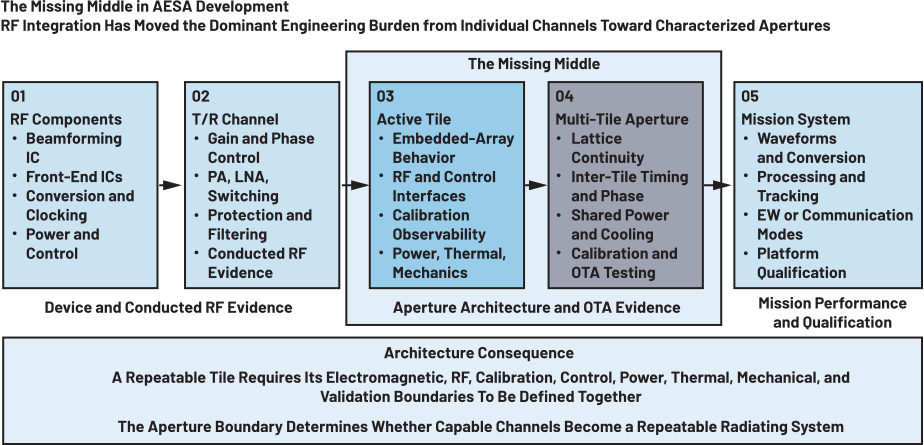
RF components and integrated transmit/receive channels provide controllable RF capability. The tile and multi-tile aperture add electromagnetic behavior, calibration, control, timing, power, thermal, mechanical, and validation responsibilities before mission-specific conversion, digitization, processing, and software are applied. The multi-tile stage represents an architecture level that allows the element count to scale.
This is the missing middle: where component-level conducted evidence gives way to the behavior of the assembled antenna aperture.
Where Component Evidence Stops
Once a channel drives a radiating element, its load is no longer the controlled impedance used on the bench. Mutual coupling makes active impedance depend on the commanded state of the array; the finite lattice reshapes embedded patterns near edges and tile boundaries. Phase and gain settings verified at the IC pins can therefore produce a different excitation at the antenna aperture—and a different beam.
Nor does every failure look like an antenna problem. A heat spreader may support an RF cavity mode, while a connector or transition adds assembly-dependent phase. A correct bias sequence can still produce the wrong aperture state when the beam command, channel map, and calibration table disagree. At this boundary, circuit, power, timing, thermal, and mechanical decisions are inseparable.2
An experienced team can quickly tune one prototype. Production asks whether its aperture behavior survives another build, thermal condition, and test station. Repeating the tile PCB proves artwork repeatability; scaling the antenna aperture also requires controlled boundaries, correction states, timing, heat flow, and mechanical registration.
Commercial leverage appears only when that discipline travels with the hardware. If every customer must rediscover intertile offsets, cooling sensitivities, timing assumptions, and part acceptance methods, the engineering remains bespoke. A useful building block separates reusable work from configuration-specific verification. That distinction matters in high-mix, low-volume aerospace and defense markets: otherwise independent missions can share hardware, calibration flows, test infrastructure, and production learning while retaining mission-specific aperture size, power, and processing.
Building a Modular X-Band AESA Aperture
The ADSY2301 makes that boundary tangible. Its 4 × 4 active tile combines 16 radiating elements with beamforming and front-end electronics. Four tiles form the demonstrated 8 × 8, 64-element aperture with shared conversion, control, power, thermal, and mechanical infrastructure (Figure 2).
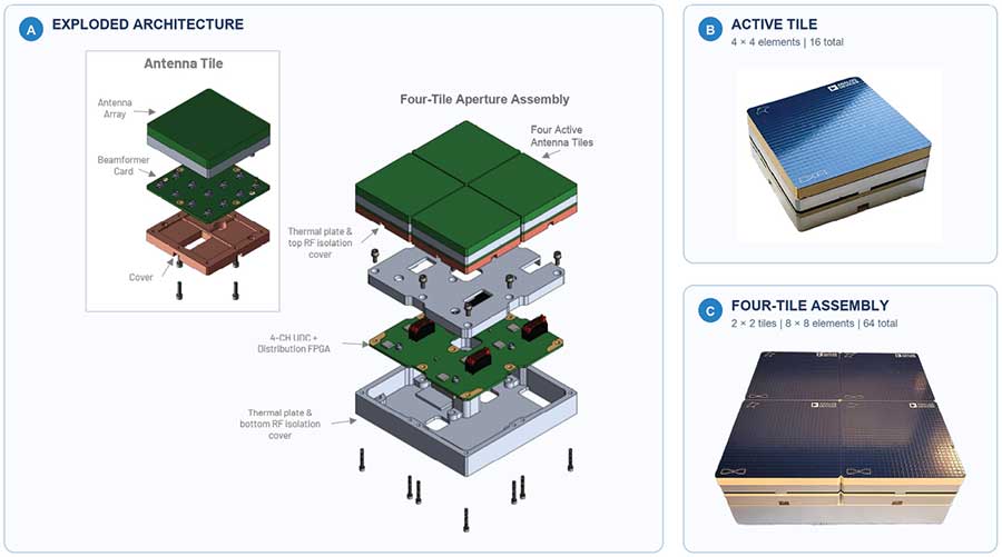
Start at the aperture face in Figure 2. The exploded architecture and photographs of the demonstrated hardware show the relationship among the 16-element active tile, beamforming electronics, RF isolation and thermal structures, frequency-conversion and control hardware, and the mechanical interfaces used to create the demonstrated 64-element assembly. Other aperture scales may repeat the active tile, the four-tile assembly, or both, where each resulting configuration requires aperture-level verification. The lattice sits directly above the beamforming card to keep RF paths short. Beneath it, the RF isolation and thermal structure control the electromagnetic environment while conducting heat into the assembly. In the four-tile configuration, this stack repeats above common conversion and control hardware. The result is not simply an antenna PCB, but a defined physical integration boundary.
The four-tile arrangement tests whether the 4 × 4 building block retains its interfaces after one level of repetition. Modular does not mean arbitrary rearrangement with unchanged performance. It means the 4 × 4 tile and four-tile assembly each present known RF, control, thermal, mechanical, and calibration interfaces that can be carried into a larger aperture. This does not eliminate all system-level assembly risks. New edge conditions, cooling loads, and calibration states must still be verified at array level for each final configuration. However, it now proceeds with an established and validated building block.
Configuration-specific validation remains necessary because every element sees an active impedance set by the excitation of the array. Frequency, scan direction, edge location, and neighboring structures all change that impedance, affecting delivered power and the combined pattern. Calibration can correct observable amplitude and phase error in the applied excitation; it cannot remove active mismatch or mutual coupling from the antenna physics.
Locating RF electronics near the elements shortens interconnects and reduces path uncertainty, but density raises coupling, narrows layout margin, and makes temperature part of RF performance and reliability.
Heat is an RF variable.
The tile cannot own platform cooling, but it can define the handoff. A mounting surface, thermal load, and conduction path let the system designer size a cold plate or enclosure without reopening the RF stack. Mechanical registration serves the aperture geometry in the same way, aligning the lattice, circuit cards, and thermal surfaces across the assembly.
Once those internal relationships are controlled, the next question is where the aperture platform should stop.
Where the Aperture Platform Ends
The aperture platform should stop before the mission-specific system, and neither the tile nor four-tile assembly should prescribe one array configuration. A compact sensor and long-range surveillance radar may use the same architecture with different counts or arrangements. Aperture area, RF power, cooling, scan requirements, and accessible channel count will change; a signals intelligence (SIGINT) receiver or communications terminal will strike another balance.
Flexibility therefore has two dimensions. Physical partitioning selects the number and arrangement of tiles or four-tile assemblies; signal-chain partitioning selects the analog subarray paths exposed to the back end. The integrator remains free to choose waveform, converters, processing, and application logic. Array-dependent functions stay with the reusable subsystem: analog beamforming, reference distribution, calibration access, control, power conditioning, and the thermal interface.
The ADSY2301 demonstrates one point in that space. The four-tile assembly exposes four controllable analog subarrays to shared frequency-conversion hardware, while common reference, control, and power functions serve the aperture. Figure 3 identifies the external back-end boundary.
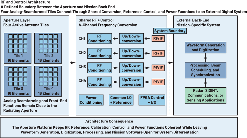
Figure 3 also makes the channel-partition trade visible. In the demonstrated four-tile configuration, four active antenna tiles connect through shared frequency conversion, reference distribution, FPGA-based control, and power conditioning to a defined external back-end boundary. The system-specific waveform, digitization, processing, and mission functions remain outside the aperture platform. Other missions may choose a different number or arrangement of tiles or four-tile assemblies, subarray partition, or back end. Combining more elements per analog subarray lowers converter count, data movement, and back-end power. Preserving more independent paths increases conversion and synchronization burden but retains calibration observability and spatial degrees of freedom for interference suppression or future modes. The mission sets both the physical aperture and the channels presented to the back end; the platform should expose that trade, not silently fix it.
A programmed phase state is not yet a beam. Hardware addresses, array coordinates, state timing, synchronization, and calibration must agree. The beam record also needs frequency, transmit/receive mode, taper, quantized state, and calibration revision. Keeping that context with the tile identity makes a command reproducible after power cycling or assembly changes.
Calibration therefore begins in the hardware architecture. Algorithms can correct only errors exposed through stable command states, known references, observable channels, and metrics tied to the radiated result. Conducted paths make selected corrections efficient; over-the-air (OTA) measurements reveal what antenna, electronics, mechanics, and environment do together. Loopback access, reference channels, synchronization, and software-visible correction states must exist before an algorithm can use them.3
With that platform boundary defined, scalability becomes a concrete question: can multiple tiles preserve one electrical and calibration frame after assembly?
Scaling a Modular Tile into a Coherent Aperture
The measured four-tile assembly provides the scalability evidence available here. Four 4 × 4 tiles establish an 8 × 8 geometry, but element count alone does not create a coherent aperture. Lattice continuity, common references, coordinate conventions, and relative correction states must place all 64 channels in one electrical frame.
Assembly exposes hidden errors: cable and transition differences shift phase and amplitude; thermal paths give adjacent tiles different histories; an edge element enters a new coupling environment when its neighbor is installed. The assembled aperture must absorb these changes without losing beam control.
The calibration hierarchy follows the hardware. Channel characterization establishes controllable RF behavior; tile calibration aligns elements within a subarray; aperture alignment resolves relative tile offsets and verifies the combined beam. Keeping these levels distinct separates local defects from assembly errors.
Over-the-air measurement closes the evidence chain. Earlier ADI work used radiated patterns to connect channel and subarray calibration to a 32-element hybrid-beamforming aperture.4 For the ADSY2301, the four-tile array was calibrated OTA and measured on a far-field range.5 At 10GHz, a mechanical gimbal swept azimuth while electronic beams were commanded from –60° to +60° in 15° increments. Figure 4 shows the normalized patterns.
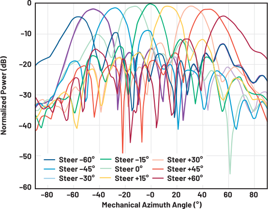
Figure 4 answers a narrow but essential question: does the calibrated 64-element assembly form and steer a main beam across these commands? It does. The common reference preserves relative peak differences, but it is not an absolute transmit budget; one frequency and azimuth cut cannot establish the full scan volume or environmental and production stability. A comprehensive OTA data package will be available for download; those stability claims require separate qualification.
This evidence is bounded to the 64-element configuration. Although both the 4 × 4 tile and four-tile assembly can serve as units in larger AESAs, changing panel size or back-end partition alters edge population, distribution lengths, cooling load, and calibration. Interfaces and the validation hierarchy carry forward; coherent beam performance, thermal margin, and calibration stability must be re-established.
What Becomes Reusable
The reusable result is not one 4 × 4 tile or 8 × 8 assembly, but a two-level architecture: two integration units plus the interfaces, calibration hierarchy, thermal and mechanical handoffs, and evidence needed to use either in a larger aperture. The ADSY2301 makes that bounded work reusable.
A program that fits the demonstrated 64-element assembly can begin waveform and range-Doppler work through a measured aperture, then move to beam scheduling, clutter rejection, and tracking. Another may add tiles, repeat four-tile assemblies, or choose different physical and channel partitions. Both start from known units and interfaces, then verify the electromagnetic, thermal, calibration, and OTA behavior of their own configuration.
Some missions will exceed the tile’s electromagnetic, power, or mechanical limits; a custom aperture may then be the right answer. The platform’s value is exposing that decision early. Commercial leverage appears when shared hardware removes more integration work than it creates at the surrounding system boundary, allowing otherwise low-volume programs to aggregate nonrecurring engineering, tooling, calibration infrastructure, production learning, and support while differentiating above the aperture.
Greater RF integration will keep improving phased arrays, but the consequential system step is turning that capability into a predictable radiating subsystem with known interfaces and measured limits. The ADSY2301 is one X-band proof point. It integrates RF channels into a characterized antenna aperture, demonstrates calibrated beam formation in a 64-element configuration, and leaves the mission system open. The significance is not tied to one element count or panel size; it is a common two-level foundation that lets high-mix, low-volume programs share a production and calibration core while aperture size, power, cooling, channel partitioning, and back-end processing remain mission-specific.
That is the missing middle: enough common structure for commercial learning to compound, with enough open partitioning for the mission to remain in control.
References
1“Analog Devices and Keysight Technologies Join Forces to Advance the Adoption of Phased Array Technology." Analog Devices, Inc., October 2022.
2Joel Dobler and Sam Ringwood. “Overcoming Common Planar Phased Array Circuit Design Challenges.” Analog Devices, Inc., June 2023.
3Siddhartha Das and Sam Ringwood. “Calibration Implementation Techniques for Multichannel Phased Array Subsystems.” Analog Devices, Inc., May 2026.
4Sam Ringwood, Peter Delos, Michael Jones, and Michael Stetzler. “Over-the-Air Pattern Measurements for a 32-Element Hybrid Beamforming Phased Array.” Analog Devices, Inc., June 2023.
5Muhammad Hamza and Jeff Massman. “A Low-Profile X-Band Phased-Array Tile on PCB Using Wideband Tightly Coupled Dipoles.” 2026 IEEE International Symposium on Antennas and Propagation and INC/USNC‐URSI Radio Science Meeting (AP-S/ INC-USNC-URSI), July 2026.
著者について
Jeff Massman received his B.S.E. degree in electrical engineering from the U.S. Air Force Academy and M.S.E. and Ph.D. degrees from the Air Force Institute of Technology. He is chief systems architect, phased arrays, at