概要
設計リソース
設計/統合ファイル
- Schematic
- Bill of Materials
- Gerber Files
- Allegro Files
- Assembly Drawing
評価用ボード
型番に"Z"が付いているものは、RoHS対応製品です。 本回路の評価には以下の評価用ボードが必要です。
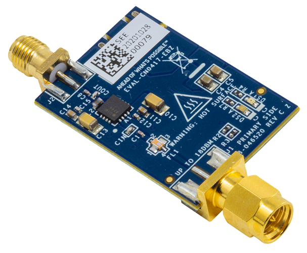
- EVAL-CN0417-EBZ ($47.38) USB Powered 2.4 GHz RF Power Amplifier
機能と利点
- +20 dB Gain Block
- USB Powered
- SMA connector for ease of use
参考資料
-
EVAL-CN0417-EBZ - User Guide2018/12/07WIKI
回路機能とその特長
Most of the modern radio-link systems capable of transmitting signals have limited output power. Depending on the environment and signal power, the range of transmission varies. For longer range of operation or environments with more RF interference, a higher output power is required. In this case, RF power amplifiers are used to increase the magnitude of power of transmitted signals to a level high enough to reach a given distance.
The circuit shown in Figure 1 is a small USB powered RF power amplifier optimized for 2400 MHz operation. The amplifier typically provides 20 dB of gain through its RF band of operation, boosting signals for various communication protocols such as ISM, MC-GSM, W-CDMA, TD-SCDMA and LTE.
It requires 5 V USB supply for normal operation. An automatic over temperature management circuit ensures that the board temperature remains within recommended operating range. The input and output, both populated with edge mounted SMA connectors, are dc blocked and matched to 50 Ω for ease of use.
回路説明
Amplifier
The ADL5606 is a broadband, two-stage, 1 W RF driver amplifier that operates over a frequency range of 1800 MHz to 2700 MHz. The device can be used in a wide variety of wired and wireless communication protocols, including ISM, MCGSM, W-CDMA, TD-SCDMA, and LTE.

The ADL5606 operates on a 5 V supply voltage and a supply current of 362 mA. The driver also incorporates a fast power up/power-down function for time division duplex (TDD) applications such as WiMAX and Wi-Fi, applications that require a power saving mode and applications that intermittently transmit data. When disabled, the ADL5606 draws approximately 4 mA of current from the power supply and 1.4 mA from the DISABLE pin.
Impedance Matching
The RF input (Pin 1) and RF outputs (Pin 9 to Pin 12) of the ADL5606 can be matched to 50 Ω with at most one external component and the microstrip line used as an inductor.
The recommended component values for ADL5606 matching are provided in the product data sheet for three frequency bands: 1960 MHz, 2140 MHz, and 2630 MHz. For this application, the recommended matching capacitances values used were from the 2630 MHz operation.

The placement of these matching capacitors are critical and is shown in Figure 3. The recommended spacing for ADL5606 matching is provided in the product data sheet for the same three frequency bands: 1960 MHz, 2140 MHz, and 2630 MHz. Again, for this application, the recommended spacing used was for the 2630 MHz operation. This was further optimized from simulations in Advanced Design System (ADS) for the desired 2400 MHz operation. Results from simulation gave 117 mils for the input matching length and 113 mils for the output matching length. The component spacing is referenced from the center of the matching component to the edge of the ADL5606.
Bandpass Filter
The input signal is filtrated by this bandpass filter centered at 2450 MHz with a 100 MHz bandwidth of operation. Figure 4 shows the electrical performance of the bandpass filter.

It has a frequency of operation from 2400 MHz to 2500 MHz, return loss of 1.5 dB maximum and return loss of 9.5 dB maximum. The maximum input power to the bandpass filter is 2 W.
USB Power Management

The circuit is powered by the 5 V VBUS voltage available on the USB port, which is then regulated by the LTM8045.
The LTM8045 is an integrated switching dc-to-dc converter that contains a current mode controller, power switching element, power coupled inductor, power Schottky diode, and a modest amount of input and output capacitance.
The device is configured as a SEPIC converter capable of accepting input voltage up to 18 V dc. The output is adjustable between 2.5 V and 15 V. It can provide approximately 430 mA at VIN = 5 V when VOUT = 5 V or −5 V.
The LTM8045 output voltage is set by connecting the feedback resistor (RFB) from VOUT+ to the FB pin. This voltage serves as the supply voltage for the amplifier ADL5606. Its value is determined from the following equation:

The LTM8045 has an operational switching frequency range between 200 kHz and 2 MHz. The switching frequency of the LTM8045 is configured using an external resistor from the RT pin to ground. Value of the eternal resistor can be determined using the following equation:

where fOSC is the typical switching frequency in MHz.
Though the LTM8045 is flexible enough to accommodate a wide range of operating frequencies, a haphazardly chosen one may result in undesirable operation under certain operating or fault conditions. A frequency that is too high can reduce efficiency, generate excessive heat, or even damage the LTM8045 in some fault conditions. A frequency that is too low can result in a final design that has too much output ripple or too large of an output capacitor.
The recommended switching frequency and resistor value for optimal efficiency over the given input and output conditions are provided in the LTM8045 data sheet. In the circuit, the RT resistor value is achieved by using two resistors in parallel to provide two places for feedback that sum together with a double filter, achieving a better filter performance.
Because the LTM8045 is a coupled inductor SEPIC, it is susceptible to large switching spikes. That is why in addition to ferrite bead at the output, an LC filter stage was for the switching spikes at 80 MHz to 150 MHz.
RF Performance
When operating the CN0417 in the 2.4GHz frequency range, the input signal is amplified from the RF input to output at a typical gain of 20 dB. Figure 6 shows the S-parameters of the circuit.

Over Temperature Management
Due to the small board size and high-power dissipation of the gain amplifier, the board could get hot beyond 85°C. Operation of the ADL5606 beyond this temperature affects its performance. To combat this issue, the circuit provides an over temperature management circuit which will automatically disable the ADL5606 amplifier upon over temperature detection, and enable it again when below a temperature threshold. It consists of a temperature switch, a non-inverting buffer, and a red LED as an indicator as shown in Figure 7. The output of this is connected to the disable pin of the ADL5606.

The ADT6402 is a push-pull output temperature switch powered by the 5V from the USB bus. Its output is active high if the temperature measured is greater than the pin-selectable trip level.
The temperature trip level and hysteresis value can be set through S0, S1 and S2 pins of the ADT6402. These three pins can be connected to VCC, tied to GND, or left floating. The ADT6402 decodes the inputs on S0, S1, and S2 to determine the temperature trip point and hysteresis value, as outlined in Figure 8. Overall accuracy for the ADT6402 is ±6°C (maximum) from −45°C to +115°C.

In this circuit, a 95°C trip point with 10°C hysteresis is selected. Hysteresis prevents oscillation on the output pin when the temperature is approaching the trip point and after the output pin is activated. Given this, the temperature reading of the ADT6402 must go as low as 85°C before the over temperature circuit output goes low, which turns on the amplifier as shown in Figure 9.

In the disabled state, the ADL5606 draws approximately 1.4 mA of current from the DISABLE pin. Since the ADT6402 is only able to source 800μA, a non-inverting buffer is used to satisfy the 1.4mA current requirement for the DISABLE pin. The buffer is also powered by the 5V from the USB bus.
Layout Considerations
Because the size of the board is quite small, the board temperature reaches approximately 85°CC around the vicinity of the ADL5606 in normal operation. To spread this heat evenly and keep the board temperature below 85°C, this design has 6 layer stack-up, the ground copper plane was made thicker at 3 oz, and more vias were added around the ADL5606 chip. Sigrity simulation, shown in Figure 10, can also be used to estimate the board temperature.

バリエーション回路
The CN0522 is designed and optimized for 915MHz band, providing a typical gain of 23dB.
For a different frequency band of operation, the ADL5604 and ADL5605 can be used. The ADL5604 is capable of a wide frequency of operation from 700 MHz to 2700 MHz, with a typical gain of 12.2 dB. The ADL5605 operates from 700 MHz to 1000 GHz at 23 dB typical gain.
Analog Devices, Inc., driver amplifiers are available in a wide range of medium power general-purpose amplifiers covering the frequency range from 400 MHz (IF) to RF microwave and W-band (86 GHz). These driver amplifiers include output power levels from 15 dBm up to approximately 1 W and covers various frequencies, bandwidths, and gain levels.
回路の評価とテスト
Equipment Needed
The following equipment is needed:
- EVAL-CN0417-EBZ circuit evaluation board
- RF signal source (RF signal generator, ADALM-Pluto)
- Micro-USB power adaptor or micro-USB to USB cable
- SMA to SMA cable
Functional Block Diagram
Figure 11 shows the functional block diagram of the test setup.

Setup and Test
- Directly connect the RF output port of the RF signal source to the EVAL-CN0417-EBZ RF input (J1).
- Connect the RF output of the EVAL-CN0417-EBZ (J2) to the RF network analyzer equipment through an SMA male to SMA male cable.
- Plug in the micro-USB cable to P1 of the EVAL-CN0417-EBZ.
- Plug the other end to a power outlet or a PC USB port.
- The EVAL-CN0417-EBZ then automatically turns on.
- Using the network analyzer, sweep the frequency from 2.2GHz to 2.6GHz and measure the S-parameters.


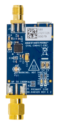
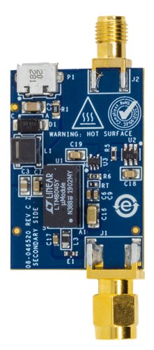
Figure 12 shows a photograph of the top side of the EVAL-CN0417-EBZ containing the ADL5606 and other RF components. Figure 13 shows the bottom side of the EVAL-CN0417-EBZ with micro-USB connector and power supply circuitry.
For complete information and details regarding test setup, see the CN0417 User Guide.


