
ADPS43506-RD Communications Power Solution


製品概要
設計リソース
説明
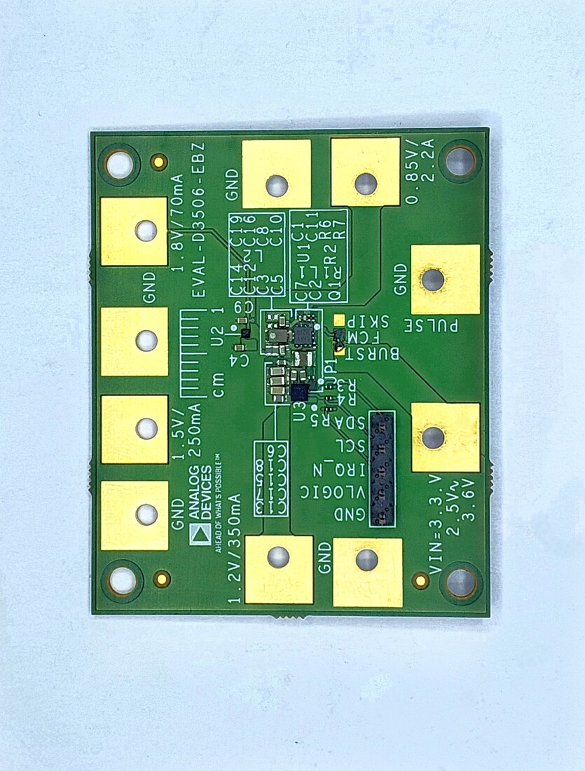
The ADPS43506-RD is a compact, efficient, high-performance system-level power solution designed for optical transceiver modules and other communications systems. The ADPS43506-RD addresses the need for multiple low-noise power rails, high efficiency, precise sequencing, and effective thermal management within limited PCB space. Leveraging ADI’s Silent Switcher® technology and SIMO architecture, the solution delivers the addressed performance while minimizing component count and board area. The validated design reduces development risk and accelerates time to market for applications including optical transceivers, telecom equipment, industrial networking, test and measurement systems, and broadband access devices.
Applications
- Optical Transceivers
- Telecom Equipment
- Industrial Networking
- Test and Measurement Systems
- Broadband Access Devices
機能と利点
- Removes existing power solutions' struggle with ripple, regulation, and load current constraints in compact form factors.
- Silent Switcher technology enables high current delivery with ultra-clean, low-noise outputs.
- SIMO architecture generates multiple rails without increasing component count or PCB footprint.
- Combined approach enables a compact, efficient, and high-performance power delivery network.
Solution Specifications
Solution Requirements:
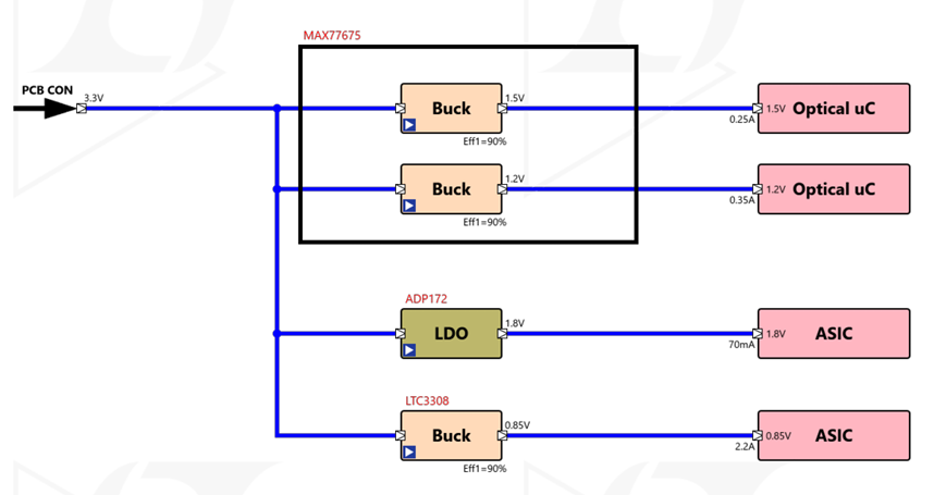
- Operates from a 3.3 V ±5% input rail and generates four output voltages (0.85 V, 1.2 V, 1.5 V, and 1.8 V) with tolerances ranging from ±3.0% to ±5.0%, ensuring regulated and stable power delivery across all rails.
- 0.85 V ± ~3.00% output voltage delivers up to 2.2 A output current with 21.25 mVpp voltage ripple.
- 1.2 V ± 5.00% output voltage provides 350 mA maximum current with 30 mVpp ripple.
- 1.5 V ± 3.33% output voltage provides 250 mA maximum current and achieves the lowest ripple performance (15 mVpp).
- 1.8 V ± 5.00% output voltage supports 70 mA maximum current with 30 mVpp ripple.
- Soft-start ramp times are 20 µs for the 0.85 V and 1.8 V rails, while the 1.2 V and 1.5 V rails start without additional programmed ramp delay.
- All rails achieve greater than 80% efficiency, with the 0.85 V rail reaching approximately 90% efficiency at 1 A load.
Environmental Requirements:
- Components -40°C to 105°C, system operation up to 85°C
Form Factor Requirements:
- PCB size 10mm x 5mm for whole power solution
No input filter is needed or any other protection. Solution is considered as Point of Load supplies.
関連資料
-
ADPS43506-RD Design Files2026/08/14ZIP18 MB
-
LTpowerCADおよびLTpowerPlanner2017/11/17
-
ADPS43506-RD LTPowerPlanner2026/08/14LTP33 KB
サポートおよびトレーニング
技術的なご質問についての回答は、ナレッジベースを検索してください。また、アナログ・デバイセズのアプリケーション・エンジニアの専任チームが、技術的なご質問にお答えいたします。