AN-2503: Quad Parametric Measurement Unit for ATE Applications using the AD5522 PMU and the AD7685 16-Bit ADC
Parametric Measurement Unit and Supporting Components
Circuit Description
The AD5522 quad PMU provides the forcing and measuring functions for the DUT, but digitizing is required external to the PMU. This can be achieved as follows:
- An ADC can be dedicated to each individual PMU channel, providing the fastest throughput and result.
- An ADC can be shared across multiple channels. In Figure 1, one AD7685 ADC is shared across the four PMU channels. In some applications, an ADC might be shared across many more channels, sometimes 8 or 16 PMU channels.
The ADC can be shared across channels using the internal Disable feature of each MEASOUTx pin. This requires a write command to the PMU register to enable/disable the appropriate switches. If this method is chosen, note that no more than one MEASOUTx channel should be selected at any one time.
Alternatively, an external 4:1 multiplexer can be used to control the measurement channel selection. In this way, all four MEASOUTx paths can be enabled, and the multiplexer makes the selection. Similarly, an 8:1 or 16:1 multiplexer would allow more measurement paths to share the one ADC. The choice of this multiplexer will depend on the ADC used and its input voltage range. For bipolar input ADCs, one member of the ADG1404/ADG1204 family would be ideal; for single-supply usage, the ADG706 and ADG708 would be more suitable. The output impedance of the MEASOUTx path is typically 60 Ω in addition to the switch impedance. Therefore, an ADC buffer, such as the ADA4898-1, should be considered to drive the ADC (buffer not shown).
The AD7685 16-bit, 250 kSPS ADC was chosen for this application because of its ability to handle the 0 V to 4.5 V output range of the MEASOUTx path. In addition, the availability of other ADCs with faster speeds in the same footprint (for example, the 16-bit, 500 kSPS AD7686) also makes it very attractive for upgrade paths.
The AD5522 requires a 5 V reference if a 20 V output range is required. The ADR435 5 V XFET reference was chosen because of its low tempco (10 ppm/°C, A Grade; 3 ppm/°C, B Grade), low noise (8 µV p-p, 0.1 Hz to 10 Hz), and ability to drive multiple PMU channels (30 mA source, 20 mA sink).
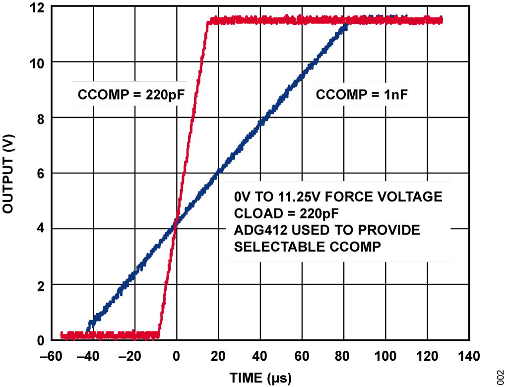
Some applications require the PMU to drive a wide range of DUT capacitances, especially applications where the PMU is connected to a power supply pin or where the PMU is used as a device power supply and will see the decoupling/bypass capacitance of the DUT. In such cases, an external switch connected to the CCOMP pin, rather than a fixed capacitor, allows for additional CCOMP capacitors to be switched in and out, thereby allowing for optimization of settling time and stability with various capacitive loads. The switch chosen for this circuit was the ADG412 quad SPST, which has an on- resistance of less than 50 Ω. The quad SPST switch was chosen instead of a multiplexer because most multiplexers allow only one of a number of channels to be on at any one time. Using the quad switch, each of the drains can be connected together and the sources connected to the each of the compensation capacitors, thereby providing 24 − 1 possible combinations of CCOMP.
Similarly, the ADG1209 differential multiplexer is used in this circuit to accommodate a wider range of feedforward capacitances connected to the CFFx pins, enabling the AD5522 to drive a wider range of DUT capacitance. The series resistance of the multiplexer used should be such that 1/(2π × RON × CDUT) > 100 kHz. In this example, the ADG1209 services two AD5522 channels.
The switch and capacitors will see the same voltage excursion as the voltage range at the FOH pin of the AD5522. Therefore, the voltage rating of the switch and capacitors should take this into account. CFF capacitors can have a ≤10% tolerance; this extra variation directly affects settling times, especially in the measure current mode for low currents. Selection of CCOMP capacitors should be ≤5% tolerance. Table 1 gives suggested nominal compensation capacitors CCOMP and CFF for various values of load capacitance.
| CLOAD | CCOMP | CFF |
| ≤1 nF | 100 pF | 220 pF |
| ≤10 nF | 100 pF | 1 nF |
| ≤100 nF | CLOAD/100 | CLOAD/10 |
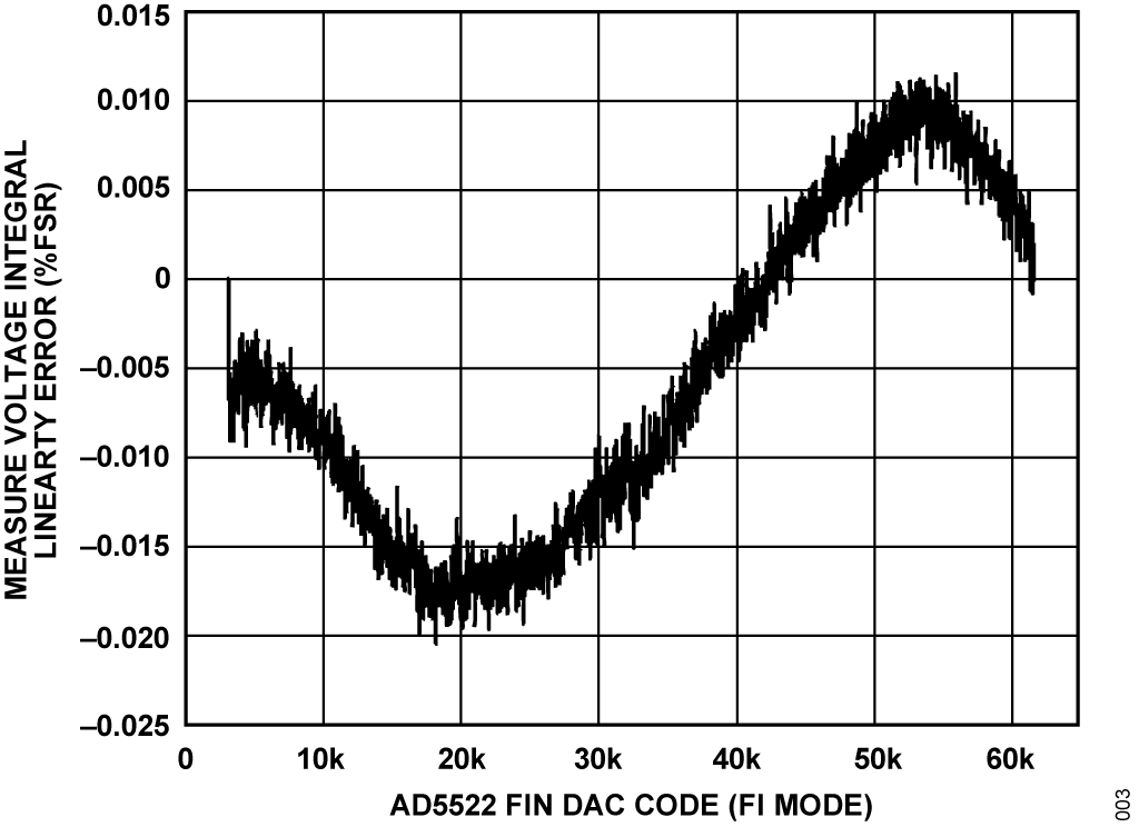
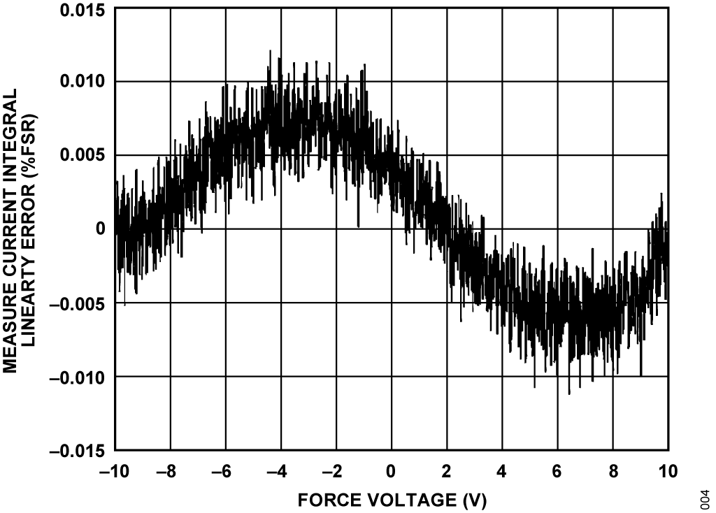
The circuit must be constructed on a multilayer PC board with a large area ground plane. Proper layout, grounding, and decoupling techniques must be used to achieve optimum performance (see Tutorial MT-031, Grounding Data Converters and Solving the Mystery of "AGND" and "DGND" and Tutorial MT-101, Decoupling Techniques). Note that Figure 1 is a simplified schematic and does not show all the necessary decoupling.
Careful consideration of the power supply and ground return layout helps to ensure the rated performance. Design the printed circuit board (PCB) on which the AD5522 is mounted so that the analog and digital sections are separated and confined to certain areas of the board. If the AD5522 is in a system where multiple devices require an AGND-to-DGND connection, the connection should be made at one point only. Establish the star ground point as close as possible to the device.
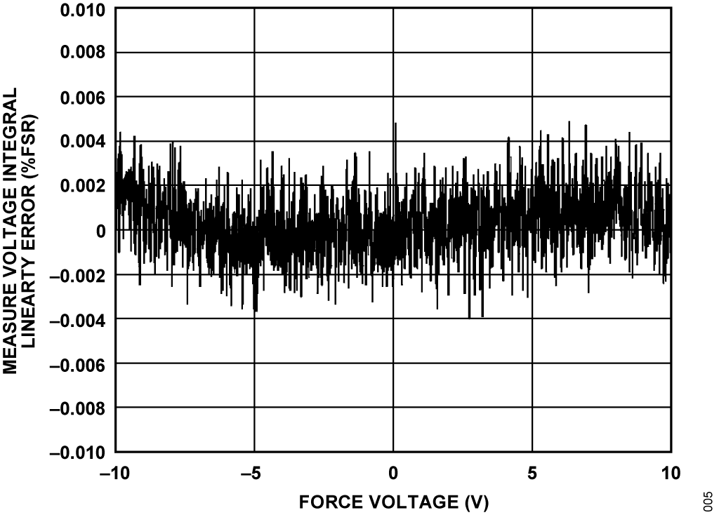
For supplies with multiple pins (AVSS and AVDD), it is recommended that these pins be tied together and that each supply be decoupled only once.
The AD5522 should have ample supply decoupling of 10 μF in parallel with 0.1 μF on each supply located as close to the package as possible, ideally right up against the device. The 10 μF capacitors are the tantalum bead type. The 0.1 μF capacitors should have low effective series resistance (ESR) and low effective series inductance (ESL)—typical of the common ceramic types that provide a low impedance path to ground at high frequencies—to handle transient currents due to internal logic switching.
Avoid running digital lines under the device because they can couple noise onto the device. However, allow the analog ground plane to run under the AD5522 to avoid noise coupling (this applies only to the package with paddle up). The power supply lines of the AD5522 should use as large a trace as possible to provide low impedance paths and reduce the effects of glitches on the power supply line. Fast switching digital signals should be shielded with digital ground to avoid radiating noise to other parts of the board, and they should never be run near the reference inputs. It is essential to minimize noise on all VREF lines.
Avoid crossover of digital and analog signals. Traces on opposite sides of the board should run at right angles to each other to reduce the effects of feedthrough through the board. As is the case for all thin packages, care must be taken to avoid flexing the package and to avoid a point load on the surface of this package during the assembly process.
Also, note that the exposed paddle of the AD5522 is connected to the negative supply, AVSS.
Common Variations
PMU circuits do not always need to use the full 20 V output range of the AD5522. Many applications require only a portion of that voltage. For example, the use of the ADR421 2.5 V voltage reference will allow the user to achieve a nominal output voltage range of ±5.6 V, which can be further scaled to suit the DUT requirements by using the on-chip OFFSET DAC. (See the AD5522 data sheet for more details). There is also the added benefit of being able to use lower supply rails. This helps by reducing the power dissipated in the AD5522, especially when operating at the full 80 mA current range per channel.
Variations in terms of the partitioning of PMU measurement channels per ADC channel could mean that one ADC channel is shared among more PMU channels (sometimes in 8:1 or 16:1 ratios).
Alternatively, the on-chip MEASOUT disable feature or an analog multiplexer can be used for this function. Multiplexers add more series resistance to the measurement path; therefore, buffering may be required prior to the ADC input.
Other variations include the use of ADCs, which handle bipolar signal ranges, or ADCs with faster sampling rates.
