MAX16610

新規設計に推奨

Switched Tank Converter (STC) Controller with Integrated Drivers

Industry's First Integrated STC that Maximizes Efficiency and Reliability with Adaptation Alogorithm

Viewing:
利用上の注意

本データシートの英語以外の言語への翻訳はユーザの便宜のために提供されるものであり、リビジョンが古い場合があります。最新の内容については、必ず最新の英語版をご参照ください。

なお、日本語版のデータシートは基本的に「Rev.0」(リビジョン0)で作成されています。そのため、英語版が後に改訂され、複数製品のデータシートがひとつに統一された場合、同じ「Rev.0」の日本語版のデータシートが異なる製品のデータシートとして表示されることがあります。たとえば、「ADM3307E」の場合、日本語データシートをクリックすると「ADM3311E」が表示されます。これは、英語版のデータシートが複数の製品で共有できるように1本化され、「ADM3307E/ADM3310E/ADM3311E/ADM3312E/ADM3315E」(Rev.J)と改訂されたからで、決して誤ってリンクが張られているわけではありません。和文化されたデータシートを少しでも有効に活用していただくためにこのような方法をとっておりますので、ご了解ください。

アナログ・デバイセズ社は、提供する情報が正確で信頼できるものであることを期していますが、その情報の利用に関して、あるいはその利用によって生じる第三者の特許やその他の権利の侵害に関して一切の責任を負いません。また、アナログ・デバイセズ社の特許または特許の権利の使用を明示的または暗示的に許諾するものでもありません。仕様は予告なしに変更する場合があります。本紙記載の商標および登録商標は、各社の所有に属します。

製品情報

  • High Density and Simplified Design
    • Integrated Drivers for 10 FETs
    • Integrated Floating Domains Generation
  • Efficiency Optimization Regardless of Component Variation
    • Adaptive On-Time Algorithm Ensures ZCS
    • Support for Wide Range of Baseline Resonant Frequencies
  • Higher Reliability
    • Adaptive Algorithm Enforces a Minimum Off Time
    • Prevents Component Over-Stress and Excessive Peak Currents
  • Protection Features
    • Input Overcurrent Protection (Latching)
    • Output Overvoltage Protection
      • Soar Mitigation and OVP
    • Bias-Supply Undervoltage Protection
    • Component Failure Protection
    • Fault/Output Voltage Indicators
      • Critical Fault-Flag Output Pin
      • Power Good Indicator
MAX16610
Switched Tank Converter (STC) Controller with Integrated Drivers
pdp-image-unavailable
myAnalogに追加

myAnalogの製品セクション(通知受け取り)、既存/新規プロジェクトに製品を追加する。

新規プロジェクトを作成
質問する
サポート

アナログ・デバイセズのサポート・ページはアナログ・デバイセズへのあらゆるご質問にお答えするワンストップ・ポータルです。


ドキュメント

データシート 1

秘密保持契約(NDA)をリクエスト

技術文書一式は、秘密保持契約(NDA)の締結後にご利用いただけます。

秘密保持契約(NDA)をリクエスト
さらに詳しく
myAnalogに追加

myAnalogのリソース・セクション、既存/新規プロジェクトにメディアを追加する。

新規プロジェクトを作成

ソフトウェア・リソース

必要なソフトウェア/ドライバが見つかりませんか?

ドライバ/ソフトウェアをリクエスト

評価用キット

eval board
MAX16610AW5EVKIT

Evaluation Kit for the MAX16610 and MAX16610A
機能と利点

  • High-Density Optimized Design
    • 3x3 Low RDSON Power MOS
    • 12-Layer Layout
    • Hot Swap and Bias Power Supply Already Implemented
  • Highly Efficient Solution
    • Low-Profile Inductors Optimized for STC Resonant Application
    • No Transformers Required
    • Resonant ZCS (Zero-Current Switching) with Adaptative Algorithm
  • Cost-Effective Solution
    • Low-ESR, Low-Cost Capacitors (No Low-Value, Low-Tolerance U2J Ceramic Capacitors have been used)
    • Integrated Gate Driving
    • Integrated Floating Power Supply for All 10 Power FETs
    • No Heat Sink is Required (Air Flow Only for Higher TDP)
  • Protection Features
    • Input Peak Overcurrent Protection
    • Output Overvoltage Protection with SOAR Mitigation
    • Input Overvoltage Protection
    • Bias and Gate Driving Undervoltage Lockout
    • Fault Flag Open Collector Signal Pin
    • Power-Good Signal
  • High-Current Output Connector Compatible with Maxim Second Stage Solution EV Kit
  • Output Adapter Board Available for a Stand-Alone Test Bench Use
  • Proven PCB Layout
  • Fully Assembled and Tested

製品詳細

The MAX16610/MAX16610A evaluation kits (EV kits) are fully assembled and tested boards that provide a working solution to evaluate the MAX16610.

The MAX16610 IC is an integrated controller packaged into a 64-pin, 9mm x 9mm TQFN. The controller generates all the gate signals required for 10 switches in a 4-to-1 switched tank converter (STC) topology. The STC is a highly efficient resonant nonisolated converter that provides voltage conversion from a 40V to 60V high-voltage bus input to a lower nonregulated DC bus output. The MAX16610/MAX16610A EV kits are designed to provide an already optimized and ready-to-use boards to evaluate the STC converter topology. The EV kits are suitable to show the full functionality of the MAX16610/MAX16610A STC controller and as well give important design rules and suggestions to implement the solution on a custom system board.

All components have been selected and optimized to achieve the best trade-off between performance, size, and overall cost. The EV kits have been developed through an accurate 12-layer PCB (plus top and bottom) layout with all the active devices on the top layer. They are designed to minimize noise and maximize converter efficiency. Test points are available on the board to probe signals useful during the evaluation of the solution. Layout source files are available and can be provided upon request. For full IC information, refer to the MAX16610/MAX16610A data sheet.

Warning: The EV kits are designed to operate with 40V to 60V DC input voltage. High voltage and high current are present in this application. Follow safe procedures when working with high-current electrical equipment.
Under severe fault or failure conditions, these EV kits can dissipate a large amount of power, which could result in mechanical ejection of the component debris at high velocity. Operate the EV kits with care to avoid possible injury.

Assembly Option

This document is common to both MAX16610GTB+ and MAX16610AGTB+ EV kits and can be used as a technical guide to test both solutions.

Two different EV kits order codes are available. On the silk top, an assembly option is marked to distinguish the two EV kits.

  • MAX16610AW5EVKIT#
    • This EV kit is dedicated to MAX16610AGTB+, marked as assy option 02
  • MAX16610#W5EVKIT#
    • This EV kit is dedicated to MAX16610GTB+, marked as assy option 01

MAX16610 vs MAX16610 Features

The two MAX16610x part numbers differ only for one protection feature.

The MAX16610 has enabled a VOUT timeout protection. This protection feature generates a fault condition that immediately stops any PWM signal if a longer time than 150ms elapses between the EN (enable) signal rising edge and VOUT level > 1V. This protects the converter against any malfunction or misbehavior of its upstream hot-swap converter or load. The 5V bias supply needs to be recycled if a VOUT timeout trips.

The MAX16610A does not support this timeout protection mechanism. Refer to the MAX16610/MAX16610A data sheet for further information on VOUT timeout protection.

eval board
MAX16610-W5EVKIT

Evaluation Kit for the MAX16610 and MAX16610A
機能と利点

  • High-Density Optimized Design
    • 3x3 Low RDSON Power MOS
    • 12-Layer Layout
    • Hot Swap and Bias Power Supply Already Implemented
  • Highly Efficient Solution
    • Low-Profile Inductors Optimized for STC Resonant Application
    • No Transformers Required
    • Resonant ZCS (Zero-Current Switching) with Adaptative Algorithm
  • Cost-Effective Solution
    • Low-ESR, Low-Cost Capacitors (No Low-Value, Low-Tolerance U2J Ceramic Capacitors have been used)
    • Integrated Gate Driving
    • Integrated Floating Power Supply for All 10 Power FETs
    • No Heat Sink is Required (Air Flow Only for Higher TDP)
  • Protection Features
    • Input Peak Overcurrent Protection
    • Output Overvoltage Protection with SOAR Mitigation
    • Input Overvoltage Protection
    • Bias and Gate Driving Undervoltage Lockout
    • Fault Flag Open Collector Signal Pin
    • Power-Good Signal
  • High-Current Output Connector Compatible with Maxim Second Stage Solution EV Kit
  • Output Adapter Board Available for a Stand-Alone Test Bench Use
  • Proven PCB Layout
  • Fully Assembled and Tested

製品詳細

The MAX16610/MAX16610A evaluation kits (EV kits) are fully assembled and tested boards that provide a working solution to evaluate the MAX16610.

The MAX16610 IC is an integrated controller packaged into a 64-pin, 9mm x 9mm TQFN. The controller generates all the gate signals required for 10 switches in a 4-to-1 switched tank converter (STC) topology. The STC is a highly efficient resonant nonisolated converter that provides voltage conversion from a 40V to 60V high-voltage bus input to a lower nonregulated DC bus output. The MAX16610/MAX16610A EV kits are designed to provide an already optimized and ready-to-use boards to evaluate the STC converter topology. The EV kits are suitable to show the full functionality of the MAX16610/MAX16610A STC controller and as well give important design rules and suggestions to implement the solution on a custom system board.

All components have been selected and optimized to achieve the best trade-off between performance, size, and overall cost. The EV kits have been developed through an accurate 12-layer PCB (plus top and bottom) layout with all the active devices on the top layer. They are designed to minimize noise and maximize converter efficiency. Test points are available on the board to probe signals useful during the evaluation of the solution. Layout source files are available and can be provided upon request. For full IC information, refer to the MAX16610/MAX16610A data sheet.

Warning: The EV kits are designed to operate with 40V to 60V DC input voltage. High voltage and high current are present in this application. Follow safe procedures when working with high-current electrical equipment.
Under severe fault or failure conditions, these EV kits can dissipate a large amount of power, which could result in mechanical ejection of the component debris at high velocity. Operate the EV kits with care to avoid possible injury.

Assembly Option

This document is common to both MAX16610GTB+ and MAX16610AGTB+ EV kits and can be used as a technical guide to test both solutions.

Two different EV kits order codes are available. On the silk top, an assembly option is marked to distinguish the two EV kits.

  • MAX16610AW5EVKIT#
    • This EV kit is dedicated to MAX16610AGTB+, marked as assy option 02
  • MAX16610#W5EVKIT#
    • This EV kit is dedicated to MAX16610GTB+, marked as assy option 01

MAX16610 vs MAX16610 Features

The two MAX16610x part numbers differ only for one protection feature.

The MAX16610 has enabled a VOUT timeout protection. This protection feature generates a fault condition that immediately stops any PWM signal if a longer time than 150ms elapses between the EN (enable) signal rising edge and VOUT level > 1V. This protects the converter against any malfunction or misbehavior of its upstream hot-swap converter or load. The 5V bias supply needs to be recycled if a VOUT timeout trips.

The MAX16610A does not support this timeout protection mechanism. Refer to the MAX16610/MAX16610A data sheet for further information on VOUT timeout protection.

eval board
MAX16610ADPEVKIT

Evaluation Kit for the MAX16610 and MAX16610A

機能と利点

  • High-Density Optimized Design
    • 3x3 Low RDSON Power MOS
    • 12-Layer Layout
    • Hot Swap and Bias Power Supply Already Implemented
  • Highly Efficient Solution
    • Low-Profile Inductors Optimized for STC Resonant Application
    • No Transformers Required
    • Resonant ZCS (Zero-Current Switching) with Adaptative Algorithm
  • Cost-Effective Solution
    • Low-ESR, Low-Cost Capacitors (No Low-Value, Low-Tolerance U2J Ceramic Capacitors have been used)
    • Integrated Gate Driving
    • Integrated Floating Power Supply for All 10 Power FETs
    • No Heat Sink is Required (Air Flow Only for Higher TDP)
  • Protection Features
    • Input Peak Overcurrent Protection
    • Output Overvoltage Protection with SOAR Mitigation
    • Input Overvoltage Protection
    • Bias and Gate Driving Undervoltage Lockout
    • Fault Flag Open Collector Signal Pin
    • Power-Good Signal
  • High-Current Output Connector Compatible with Maxim Second Stage Solution EV Kit
  • Output Adapter Board Available for a Stand-Alone Test Bench Use
  • Proven PCB Layout
  • Fully Assembled and Tested

製品詳細

The MAX16610/MAX16610A evaluation kits (EV kits) are fully assembled and tested boards that provide a working solution to evaluate the MAX16610.

The MAX16610 IC is an integrated controller packaged into a 64-pin, 9mm x 9mm TQFN. The controller generates all the gate signals required for 10 switches in a 4-to-1 switched tank converter (STC) topology. The STC is a highly efficient resonant nonisolated converter that provides voltage conversion from a 40V to 60V high-voltage bus input to a lower nonregulated DC bus output. The MAX16610/MAX16610A EV kits are designed to provide an already optimized and ready-to-use boards to evaluate the STC converter topology. The EV kits are suitable to show the full functionality of the MAX16610/MAX16610A STC controller and as well give important design rules and suggestions to implement the solution on a custom system board.

All components have been selected and optimized to achieve the best trade-off between performance, size, and overall cost. The EV kits have been developed through an accurate 12-layer PCB (plus top and bottom) layout with all the active devices on the top layer. They are designed to minimize noise and maximize converter efficiency. Test points are available on the board to probe signals useful during the evaluation of the solution. Layout source files are available and can be provided upon request. For full IC information, refer to the MAX16610/MAX16610A data sheet.

Warning: The EV kits are designed to operate with 40V to 60V DC input voltage. High voltage and high current are present in this application. Follow safe procedures when working with high-current electrical equipment.
Under severe fault or failure conditions, these EV kits can dissipate a large amount of power, which could result in mechanical ejection of the component debris at high velocity. Operate the EV kits with care to avoid possible injury.

Assembly Option

This document is common to both MAX16610GTB+ and MAX16610AGTB+ EV kits and can be used as a technical guide to test both solutions.

Two different EV kits order codes are available. On the silk top, an assembly option is marked to distinguish the two EV kits.

  • MAX16610AW5EVKIT#
    • This EV kit is dedicated to MAX16610AGTB+, marked as assy option 02
  • MAX16610#W5EVKIT#
    • This EV kit is dedicated to MAX16610GTB+, marked as assy option 01

MAX16610 vs MAX16610 Features

The two MAX16610x part numbers differ only for one protection feature.

The MAX16610 has enabled a VOUT timeout protection. This protection feature generates a fault condition that immediately stops any PWM signal if a longer time than 150ms elapses between the EN (enable) signal rising edge and VOUT level > 1V. This protects the converter against any malfunction or misbehavior of its upstream hot-swap converter or load. The 5V bias supply needs to be recycled if a VOUT timeout trips.

The MAX16610A does not support this timeout protection mechanism. Refer to the MAX16610/MAX16610A data sheet for further information on VOUT timeout protection.

MAX16610AW5EVKIT
Evaluation Kit for the MAX16610 and MAX16610A
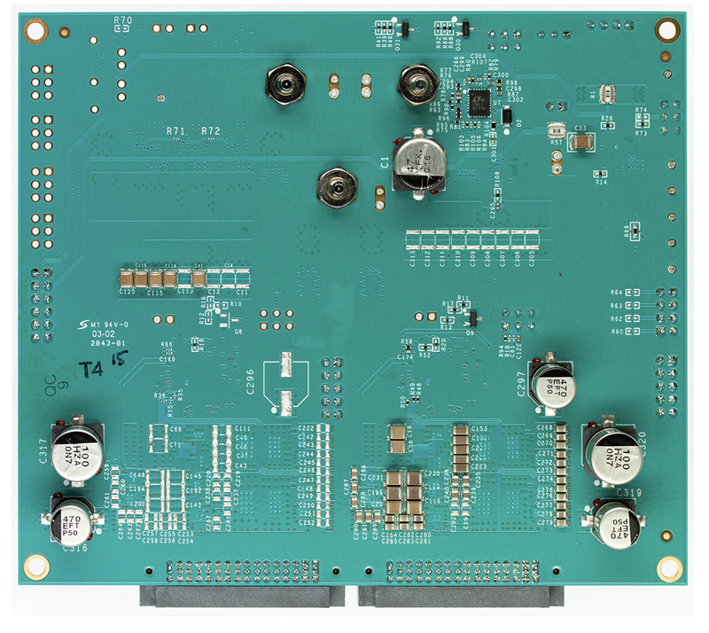
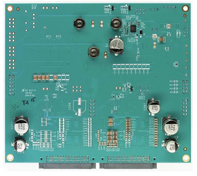
MAX16610#W5EVKIT、MAX16610ADPEVKIT、MAX16610AW5EVKIT:ボード写真
MAX16610-W5EVKIT
Evaluation Kit for the MAX16610 and MAX16610A
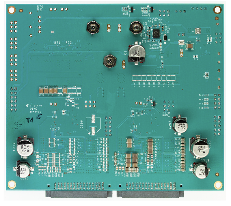
MAX16610#W5EVKIT、MAX16610ADPEVKIT、MAX16610AW5EVKIT:ボード写真
MAX16610ADPEVKIT
Evaluation Kit for the MAX16610 and MAX16610A
MAX16610#W5EVKIT、MAX16610ADPEVKIT、MAX16610AW5EVKIT:ボード写真

最新のディスカッション

MAX16610に関するディスカッションはまだありません。意見を投稿しますか?

EngineerZone®でディスカッションを始める

最近表示した製品