MAX16425
新規設計に推奨アプリケーション設定を選択可能な統合型降圧スイッチング・レギュレータ
パッケージのフットプリントを75%削減した極小レギュレータで省スペース化を実現
- 製品モデル
- 2
- 1Ku当たりの価格
- 最低価格:$4.34
製品情報
- 高効率のソリューション
- 最大ピーク効率:97%
- 全負荷時の最大効率:87%
- DCM有効時の1Aの軽負荷条件下における最大効率:96%
- フレキシブルな設計により早い段階でのPCB定義が可能
- VT2491(15A)および関連するスケーラブル製品と互換性のあるフットプリント
- 設定可能なスイッチング周波数:最大1MHz
- 設定可能なソフトスタートとSTAT遅延タイミング
- リファレンス電圧を外部入力オプションで設定可能
- 正と負のOCP制限を設定可能
- 先進のアーキテクチャ、保護、通知機能により信頼性の高い設計を実現
- 電流や温度のアナログ通知
- 差動リモート検出とオープン・サーキット検出
- Quick-PWM™アーキテクチャによる高速過渡応答
- パーセンテージ・ベースの出力パワー・グッドおよびOVP
- オープンドレイン・ステータス・インジケータ(STAT)ピン
- 入力低電圧/過電圧ロックアウト
- アダプティブ・デッド・タイム制御
- 基板スペースを節約
- 内蔵昇圧スイッチ
- 27バンプWLCSP(2.2mm x 3.8mm)フットプリント
- 入出力セラミック・コンデンサを使用した動作
MAX16425/MAX16425Aは、最大負荷25Aを要件とし、4.5V~16Vの入力電源で動作するアプリケーション向けの完全統合型高効率スイッチング・レギュレータです。これらのシングルチップ・レギュレータは、高速な過渡応答が要求される高精度出力のためのコンパクトで高効率な電力供給ソリューションを提供します。
幅広い設定に対応するため、この2つのデバイスには、異なる設定可能なオプション(詳細についてはデータシートの表3aおよび表3bを参照)が用意されています。設定可能な機能には、内部/外部リファレンス電圧、出力電圧設定値、スイッチング周波数、過電流保護レベル(OCP)、ソフトスタート・タイミングなどがあります。軽負荷時の効率を高めるために、不連続電流モード(DCM)動作をピンストラップで有効にすることができます。
MAX16425/MAX16425Aには、様々な保護機能および計測機能があります。正と負のサイクルごとのOCP、短絡保護、過熱保護(OTP)によって堅牢な設計が確保されています。入力電圧が仕様を外れたときは、入力低電圧/過電圧ロックアウトがレギュレータをシャットダウンすることで損傷を防ぎます。出力過電圧(OVP)が発生した場合はレギュレーションが停止します。出力電圧が範囲内にあること、また出力電圧がレギュレーションの範囲内にあることは、ステータス・ピンによって示されます。このデバイスにはアナログ出力があり、出力電流またはジャンクション温度をそれぞれ±5%および±8°Cの精度で通知するように設定できます。
これらのデバイスには、熱抵抗が小さく実装面積を最小限に抑える27バンプ(2.2mm x 3.8mm)WLCSPパッケージが採用されています。
アプリケーション
- サーバー/マイクロサーバー
- I/Oおよびチップセット電源
- GPUコア電源
- DDRメモリ:VDDQ、VPP、VTT
- ポイントオブロード(PoL)アプリケーション
ドキュメント
データシート 2
| 製品モデル | ピン/パッケージ図 | 資料 | CADシンボル、フットプリント、および3Dモデル |
|---|---|---|---|
| MAX16425GCJ+ | 27-ball WLCSP (Legacy Maxim) | ||
| MAX16425GCJ+T | 27-ball WLCSP (Legacy Maxim) |
これは最新改訂バージョンのデータシートです。
ソフトウェア・リソース
必要なソフトウェア/ドライバが見つかりませんか?
ドライバ/ソフトウェアをリクエスト評価用キット
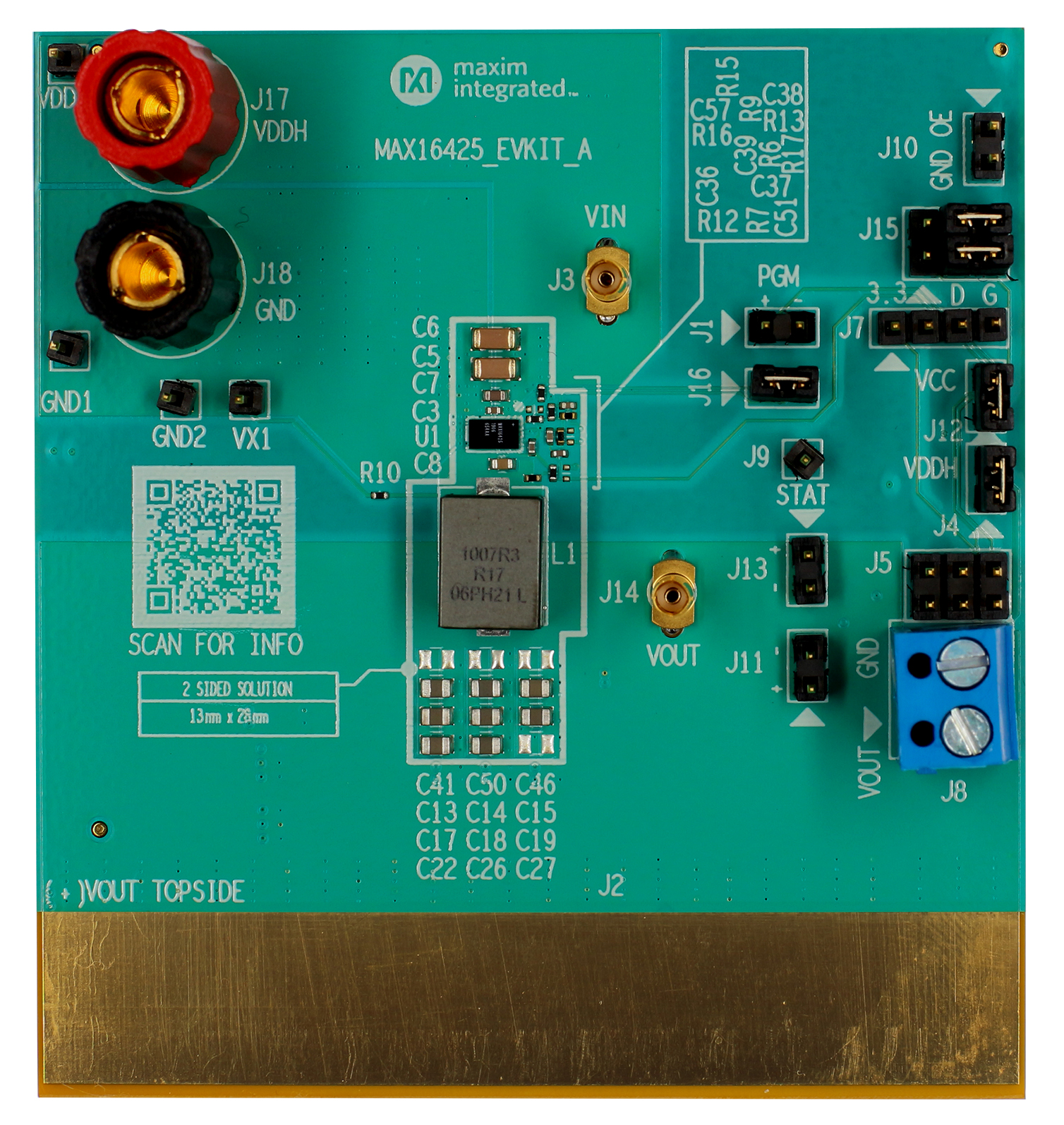
MAX16425/MAX16425Aの評価用キット
資料
最新のディスカッション
MAX16425に関するディスカッションはまだありません。意見を投稿しますか?
EngineerZone®でディスカッションを始める