ADRV9104
発売前Narrow-Band and Wideband RF Transceiver with Integrated Application Processor
製品情報
- Integrated 1 Tx × 2 Rx RF transceiver
- Operating frequency range of 70 MHz to 6000 MHz
- Transmitter and wideband receiver signal bandwidth from 12 kHzto 40 MHz
- Narrowband receiver signal bandwidth from 12 kHz to 2 MHz
- 2 fully integrated, fractional-N, RF synthesizers
- 2 fully integrated, fractional-N, RF PLLs to control external VCO banks
- Supports external LO
- LVDS and CMOS synchronous serial data interface options
- Low power monitor and sleep modes
- Fully integrated DPD for narrowband waveforms
- User-programmable ARM core with 928 kB memory
- Interfaces include 2× UART, 2× I2S, I2C, QSPI, SPI, JTAG
- Library of hardware accelerators
- Fully programmable via a 4-wire SPI
- Package: 196-ball, 10 mm × 10 mm, CSP_BGA
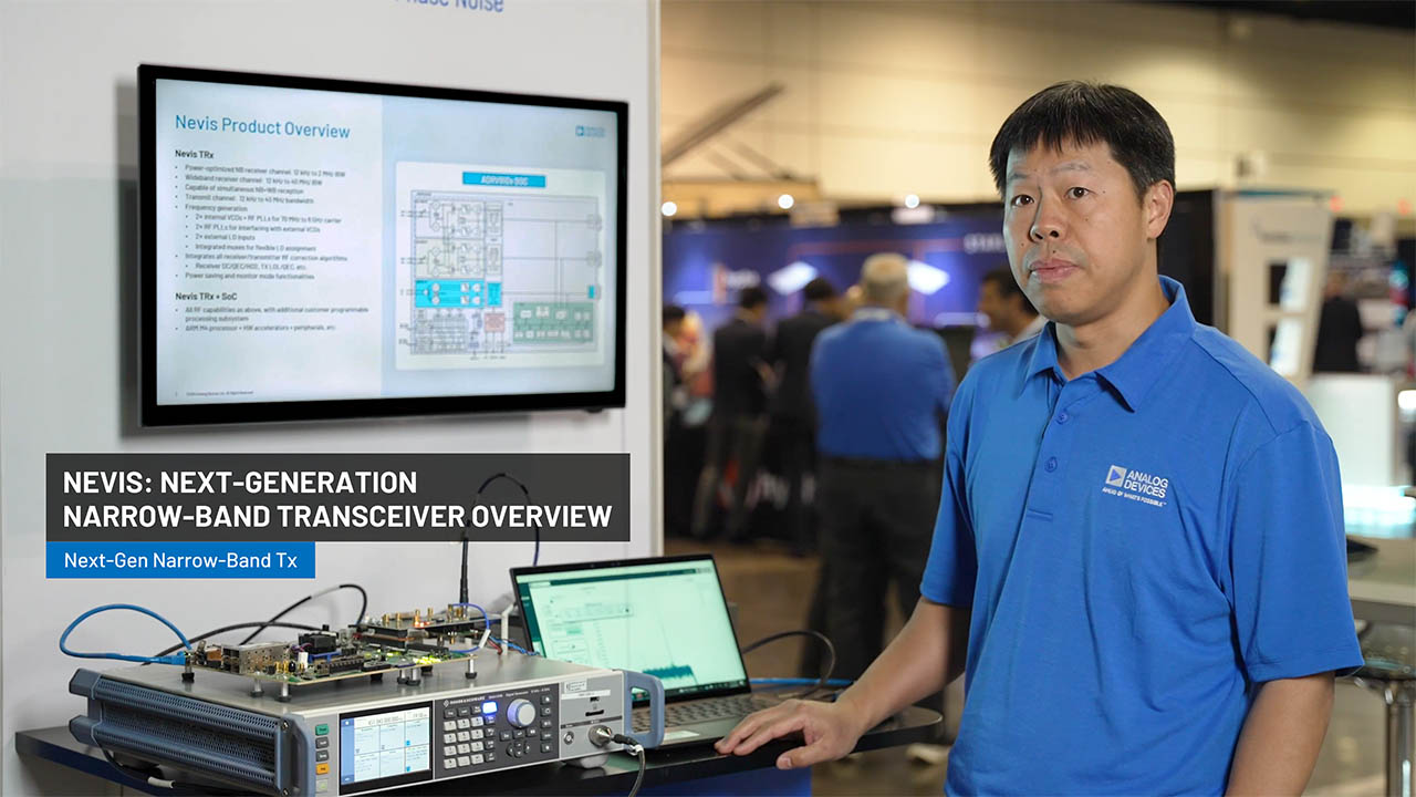
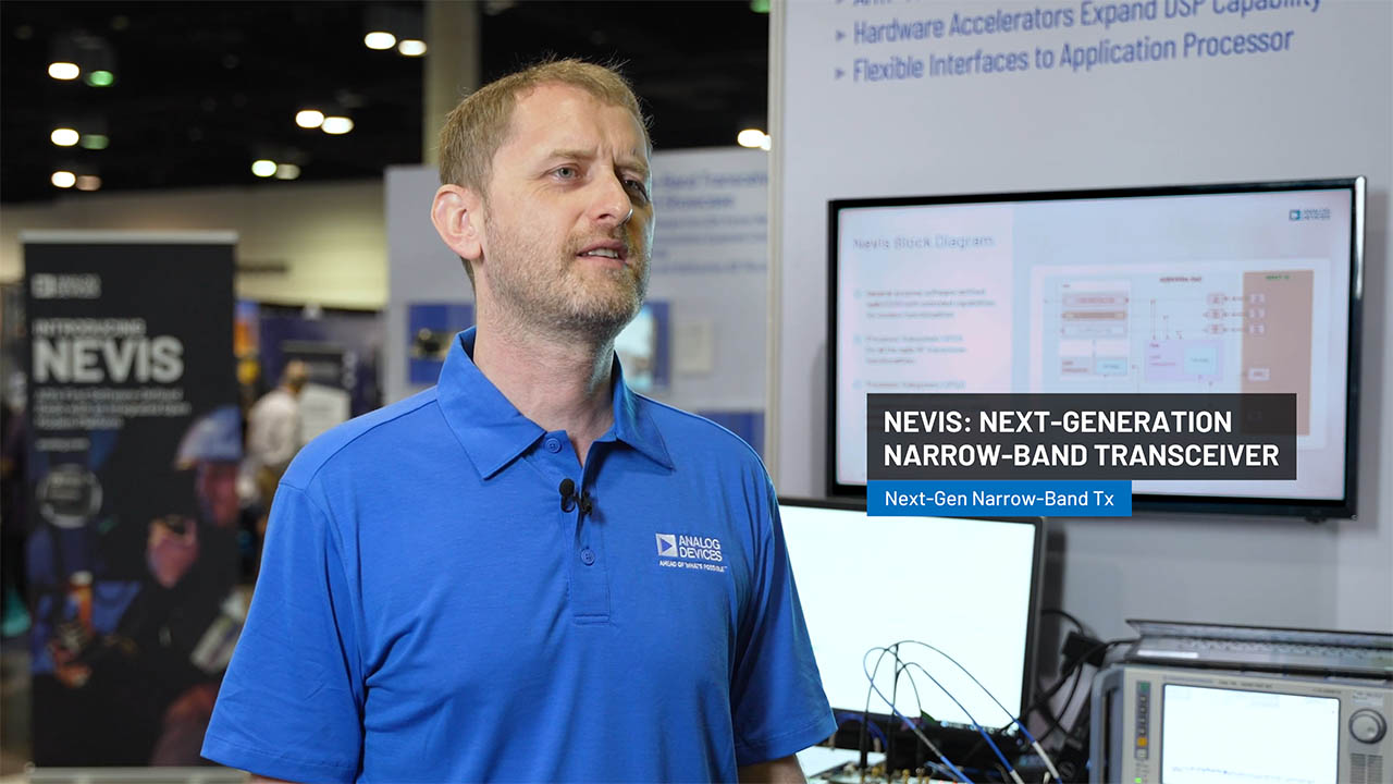
The ADRV9104 is a highly integrated RF transceiver with an integrated application processor that has a single transmitter, dual receivers, integrated synthesizers, and digital signal processing functions. Its a high performance, highly linear, high dynamic range transceiver designed for the lowest power consumption to support portable, and battery powered equipment. The ADRV9104 operates from 70 MHz to 6000 MHz and covers the VHF (from 70MHz),UHF, industrial, scientific, and medical (ISM) bands, and cellular frequency bands in narrow-band (kHz) and wideband operation up to 40 MHz. The ADRV9104 is capable of both TDD and uncalibrated FDD operation.
The transceiver has three direct conversion signal paths (1Tx and 2Rx) with state-of-the-art noise figure and linearity. The dedicated Narrow Band Receiver path can support up to 2MHz of RF signal BW. The dedicated wide band Receiver path can support up to 40MHz of RF signal BW. Each receiver and transmitter subsystem includes quadrature error correction (QEC), programmable digital filters, DC offset correction on the Rx paths and LO leakage suppression on the Tx path. In addition, functions such as analog-todigital converters (ADCs), digital-to-analog converters (DACs), and general-purpose inputs/outputs (GPIOs), are integrated to provide additional monitoring and control capability.
The transmitter has internal modulator functions that can support for typical Land Mobile Radio (LMR) standards, such as Analog FM, Digital Mobile Radio (DMR), P25. The modulator integrates the symbol mapping, interpolation and pulse shaping functions which allow the basedband processor to send 2bit symbols to ADRV9014.
The fully integrated phase-locked loops (PLLs) provide high performance, low power, fractional-N frequency synthesis for the transmitter, receiver, and clock sections. Careful design and layout techniques provide the isolation required in high performance personal radio applications.
All voltage-controlled oscillator (VCO) and loop filter components are integrated to minimize the external component count. The internal PLLs provide local oscillators (LOs) and have flexible configuration options and include fast lock modes. The fully integrated PLLs also have the option of operating with one or more external VCOs to provide ultra low noise LOs for the transmitter and receivers.
The transceiver includes low power sleep and monitor modes to save power and extend the battery life of portable devices while monitoring communications, it has the capability to monitor the DMR and Analog FM signal simultaneously with the narrow-band receiver channel when monitor mode is enabled. For some modes, ADRV9104 can operate form DEV_CLK only with the internal Clock PLL powered down.
The fully integrated, low power digital predistortion (DPD) is optimized for narrow-band TDD signals and enables linearization of high efficiency power amplifiers.
The ADRV9104 hosts a second processor, Processor Subsystem 2 (PS2), for users application specific programming. The ARM M4 has 928kB of useable memory, hardware accelerators, peripheral interfaces and runs up to 200MHz. This application processor can be used to implement modem like features on the transceiver customized to individual use cases.
The ADRV9104 core can be powered directly from 1.0 V and 1.8 V regulators and is controlled via a standard 4-wire serial port. High data rate and low data rate interfaces are supported using configurable CMOS or low voltage differential signaling (LVDS) serial synchronous interface (SSI) choice. The ADRV9104 is packaged in a 10 mm × 10 mm, 0.65 pitch 196-ball chip scale package ball grid array (CSP_BGA).
APPLICATIONS
- Land Mobile Radios
- Mobile Satellite and Satellite IoT
- Wireless microphones
- Mission critical communications systems
- Smart Meters
- Factory Automation
ドキュメント
ビデオ 2
これは最新改訂バージョンのデータシートです。