Tiny 12-Bit ADC Delivers 2.2Msps Through 3-Wire Serial Interface
Tiny 12-Bit ADC Delivers 2.2Msps Through 3-Wire Serial Interface
by
Joe Sousa
Feb 1 2000
Introduction
Serial interfaces occupy little routing space, but usually limit the speed of an ADC. The LTC1402 has a full conversion speed of 2.2Msps and a very compact 3-wire interface for connecting to DSPs and microprocessors without glue logic. It comes in a 16-pin narrow SSOP package. This minuscule package (200mil × 230mil footprint) and compact serial interface are easy to fit close to sensors to best preserve analog signal integrity.
Other serial 12-bit ADCs have sample rates limited to hundreds of kilosamples-per-second, which limits their utility in high speed data acquisition systems. This slow sample rate, combined with poor distortion characteristics, makes them unsuitable for tracking high frequency signals. The LTC1402 will capture, in less than 60ns, the fast steps from an external analog input multiplexer for high speed data acquisition and it will digitize high frequency signals very accurately, with a 72dB S/(N+D) (signal-to-noise plus distortion ratio) at 1.1MHz, for communications or signal processing systems.
3-Wire Serial Interface for DSPs, Cables and Optocouplers
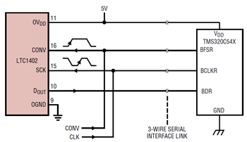
Figure 1a shows an example of interfacing the LTC1402 to the TMS320C54x DSP. No glue logic is needed to interface the LTC1402 to DSPs. The buffered serial port of the TMS320C54x talks directly to a dedicated 2kB segment of internal buffer memory. The ADC’s serial data is collected in the 2k buffer, in two alternating 1kB segments, in real time, at the full 2.2Msps conversion rate of the LTC1402. Consult the LTC1402 data sheet for the TMS320C54x assembly code for this application.

Figure 1a. DSP serial interface to the TMS320C54X.
The minuscule 16-pin narrow SSOP package of the LTC1402 saves space in compact systems or systems that require a large number of ADCs. It can be located near the signal conditioning circuitry and send serial output data over a PC board trace of up to one foot in length to the DSP, as shown in Figure 1a.
Figure 1b shows the LTC1688/LTC1520 quad cable driver/receiver interfacing the LTC1402 to the DSP port to send the serial data over longer distances. The category-5 quad twisted pair shielded cable can extend up to 100 feet without data corruption. Because the SCK, CONV and DOUT signals originate at the LTC1402, they arrive at the serial port with similar delays and remain synchronized. When the data is received at the serial port of a DSP or other processor, the port must be programmed to respond to the appropriate SCK and CONV edges. It is also necessary to check where the 12-bit output DATA sits in the 16-bit data frame. The TMS320C54x serial port READ instructions can shift the 12-bit data to the preferred position within the 16-bit data frame.

Figure 1b. The LTC1402 3-wire serial port sends data over 100 feet of category 5 twisted pair with the LTC1688/LTC1519 quad driver/receiver pairs.
The serial interface lends itself to galvanic isolation with external optocouplers. Figure 1c shows how to isolate the LTC1402 with the HPCL-2430 dual optocoupler. The 40ns propagation delays through the dual optocouplers cancel to maintain a good timing match between the DOUT, SCK and CONV signals. The LTC1402, running at a 2Msps conversion rate, sends 16-bit data frames through the HPCL-2430 optocouplers at 32MB/s.

Figure 1c. The LTC1402 is easily isolated with high speed optocouplers.
3V or 5V Serial Interface without Spurious Noise
Figure 2 shows the block diagram of the LTC1402. The internal architecture has been optimized to send out data serially during conversion, without degradation of conversion accuracy due to digital noise. The 35MHz clock input at the SCK pin (15) and the external 2.2Msps conversion start input at the CONV pin (16) do not inject noise into the internal analog signal path of the ADC. As a result, the analog accuracy of the LTC1402 is insensitive to the phase, duty cycle or amplitude (3V or 5V) of the external digital inputs. The DOUT pin (10) swings from the voltage at the OGND pin (9) to the voltage at the OVDD pin (11) to allow direct interfacing to 5V or 3V DSPs and microprocessors. The LTC1402 is ideal in multiple-ground systems, where the differential input is connected to one ground, the supplies and grounds of the LTC1402 connect to a second, local ground and the output ground connects to a third, digital ground.

Figure 2. LTC1402 block diagram.
Very High SFDR in Single 5V Supply Applications
A proprietary sampling front end circuit achieves exceptional dynamic performance at the 1.1MHz Nyquist frequency: –89dB THD with ±5V supplies and –82dB THD with a single 5V supply. Figures 3 and 4 show the spectra from a 1.1MHz Nyquist frequency sine wave with ±5V supplies and a single 5V supply, respectively. With this very clean spectrum, the LTC1402 minimizes crosstalk and interference in communications applications where the spectrum is divided into many frequency slots.

Figure 3. Sine wave spectrum plot (bipolar ±2V) with ±5V supplies.

Figure 4. Sine wave spectrum plot (unipolar 0V–4V) with single 5V supply.
The LTC1402 maintains 72dB S/(N+D) with a 1.1MHz input sine wave, with either a single 5V or ±5V supplies. Positive signals can be applied with single or dual supplies and bipolar signals are easily accommodated with dual-supply operation.
The full power bandwidth of the LTC1402 is 80MHz; the full linear bandwidths (SINAD > 68dB) of 5MHz with ±5V supplies and 3.5MHz with a single 5V supply round out the exceptional dynamic performance of the LTC1402. The wideband signal conversion purity shown in Figures 5a and 5b makes the LTC1402 well suited for digitizing sine wave signals well above the 1.1MHz Nyquist frequency. Figures 6 and 7 show that transfer function purity, represented by the differential and integral linearity plots, is maintained at the full 2.2Msps conversion rate.

Figure 5a. ENOBs and SINAD vs input frequency (bipolar ±2V) with ±5V supplies.

Figure 5b. ENOBs and SINAD vs input frequency (unipolar 0V–4V) with single 5V supply.

Figure 6. Differential nonlinearity vs output code (unipolar 0V–4V).

Figure 7. Integral nonlinearity vs output code (unipolar 0V–4V).
True Differential Inputs Cancel Wideband Common Mode Noise
The front-end sampling circuit acquires the input signal differentially from the AIN+ and AIN– analog inputs. Except for the sign inversion, these two inputs are identical. The wide common mode rejection bandwidth of the LTC1402 (–60dB at 10MHz input) affords excellent ground noise rejection in complex, noisy systems. Figure 8a shows the CMRR performance vs input frequency.

Figure 8a. CMRR vs input frequency.
The differential inputs are very easy to interface to a wide range of signal sources. Grounding the AIN– input near the signal source reduces common mode ground noise. Setting the BIP/UNI pin (8) to a logic high selects the bipolar ±2.048V range; setting it to a logic low selects the unipolar 0V to 4.096V range.
The 0V to 4.096V unipolar range is ideal for single 5V supply applications where the AIN– input is grounded and the signal is applied to the AIN+ input. The ±2.048V bipolar range centered around midsupply can also be used in single 5V supply applications, with the AIN– input tied to a 2.5VDC source. Alternately, the full ±2.048V bipolar range can be driven with a pair of complementary ±1.024V signals into AIN+ and AIN– . This limits the swing of external single 5V supply amplifiers to their most linear region, from 1.5V to 3.5V. Figure 8b shows half of the LT1813 dual op amp driving the LTC1402 in this fully differential configuration with a single 5V supply.

Figure 8b. True differential inputs accept 4VP-P bipolar differential signal with 2VP-P swings on each input and an effective gain of 2 from the LT1813 inputs. SINAD = 70.7dB with a 1MHz input.
Internal or External Reference
The internal 2.048V reference (multiplied by 2 at the VREF output) sets the bipolar and unipolar ranges to ±2.048V and 0V to 4.096V, respectively. Tying the Gain pin (7) to the VREF pin (5) cuts the reference voltage at the VREF pin and analog input spans in half, to 2.048V. The internal reference can also be disabled by tying the Gain pin to VCC and tying an external reference with an output between 2V and 5V directly to VREF.
The single-ended unipolar input range of Figure 9a’s circuit depends on the DAC’s output voltage, which acts as an infinite sample-and-hold for signals such as a CCD sensor dark current or similar applications, as determined by software procedures. The LTC1446 12-bit serial DAC applies a voltage to the GAIN and AIN– pins of the ADC, in this case subtracting the AIN– voltage from the VREF voltage, thus maintaining a positive full scale of 4.096V while varying zero scale over the range of 0V to 2V. This adjustment of the low end of the scale preserves the full 12-bit dynamic range of the ADC to digitize the input video signal between the dark-current value and 4.096V. The dark-current value must be a slow-moving DC value so that the DAC and the reference buffer amplifier can drive their respective 10µF capacitors. The LTC1446 DAC is stable with a 10µF load; care must be taken when substituting capacitors.

Figure 9a. The use of a DAC allows software adjustment of the lower end of the ADC range for applications such as dark-current cancellation.
Figure 9b shows alternative connections to emulate the functional range of a flash converter in an image scanner application. The top and bottom of the conversion ranges are set independently by the LTC1446 DAC, just like the top and bottom voltages of the internal resistor ladder in a flash converter. The bottom of the conversion range starts at the dark-current value and the top of the range is set externally to match the maximum possible output from the image scanner. The voltage at AGND (pin 6) may vary from 0V to 1V; that at VREF (pin 5) may vary from 2V to 5V. The LT1813 input buffer amplifiers may not be necessary if the image sensor has a low input impedance (<100Ω).

Figure 9b. A dual DAC allows software adjustment of both the fullscale and zero-scale voltages of the ADC, emulating the behavior of a flash converter.
Reducing Power at Low Sample Rates
The LTC1402 consumes 90mW in normal operation, on either single 5V or ±5V supplies. NAP and SLEEP modes cut back power drain to 15mW and 10mW, respectively. NAP mode leaves the reference on and takes only 300ns to wake up, making it ideal for saving power between conversions in lower-sample-rate applications. SLEEP mode also shuts down the reference and takes 10ms to wake up. The REFREADY bit in the output data stream indicates when the reference has settled to full accuracy. NAP and SLEEP modes are easily set with two or four pulses at the CONV pin (16) input, respectively. One or more pulses at the SCK pin (15) input wakes up the LTC1402 for conversion.
Figure 10 shows the reduced power consumption while the sample rate is reduced and the NAP or SLEEP modes is used between conversions. For example, an undersampling application with NAP mode between conversions at a 455ksps sample rate draws only 40mW.

Figure 10. Current consumption vs sample rates for various operating modes and supply configurations.
Conclusion
The LTC1402 has all the speed and AC and DC performance of fast 12-bit ADCs with parallel data interfaces, but it offers a much smaller, glueless serial interface that saves space in the 16-pin narrow SSOP package. The tiny LTC1402 can be placed right at the sensor for optimum analog signal capture and the compact 3-wire serial interface can be routed through a system board, through a cable or through an isolation barrier, to serial ports on DSPs and other processors.


