15V, 2.5A Monolithic Buck-Boost DC/DC Converter with 95% Efficiency and Low Noise Operation
15V, 2.5A Monolithic Buck-Boost DC/DC Converter with 95% Efficiency and Low Noise Operation
by
Eddy Wells
Jul 1 2012
Power-hungry handheld devices and industrial instruments often require multicell or high capacity batteries to support their ever-increasing processing needs. A wide voltage range, high efficiency buck-boost DC/DC converter is the ideal solution for longer battery run times and handling multiple input sources. The LTC3112 is a 2.2V to 15V input capable 2.5A buck-boost converter. The extended voltage range allows conversion from a variety of power sources such as one, two or three Li-ion cells, lead acid batteries, supercapacitors, USB cables and wall adapters to output voltages programmed between 2.5V and 14V.
The LTC3112 features the latest generation buck-boost PWM control scheme, effectively eliminating jitter when crossing the barrier between buck and boost operation. Safeguards such as current limit, overvoltage protection, thermal shutdown, and short-circuit protection provide robust operation in harsh environments.
For demanding applications where component size or conversion efficiency is critical, the LTC3112’s 750kHz default switching frequency can be synchronized between 300kHz and 1.5MHz. For designs where output current needs to be controlled or measured, an output current monitor pin is available. Selectable Burst Mode® operation extends the operating life when the battery-powered device is idle.
The LTC3112-based converter shown in Figure 1 can generate 30W of power with a 12V output. The solution footprint is less than 200mm2, which cannot be matched by a controller-based buck-boost or complex dual-inductor SEPIC design at similar power levels. The main external components are limited to the input and output filter caps and the power inductor. The LTC3112 is offered in a thermally enhanced 16-lead 4mm × 5mm DFN or 20-lead TSSOP package.

Figure 1. LTC3112 based 30W solution.
Operation from Multiple Input Sources
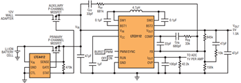
The LTC3112’s wide operating range allows devices to be powered from multiple input sources. Figure 2 shows an application where the LTC4412 PowerPath controller (TSOT-23 package) provides a low loss selection between two input sources. The LTC4412 maintains a 20mV forward voltage across the selected P-channel MOSFET, keeping losses to a minimum. In this circuit, the LTC4412 automatically switches the greater of a single Li-ion cell or 12V wall adapter to the input of the LTC3112.

Figure 2. LTC4412 PowerPath controller selects highest voltage input to power the LTC3112 converter.
Efficiency curves based on the two input sources are given in Figure 3. Peak efficiencies of greater than 90% are achieved with either input. Selectable Burst Mode operation (dashed lines) with 50µA of typical sleep current extends high efficiency operation for more than two decades of load current.

Figure 3. 5V output efficiency from a single Li-ion cell (3.6V) or wall plug (12V).
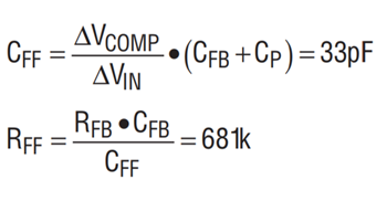
A feedforward network (CFF, RFF of Figure 2) connected between the VIN and FB pins provides improved transient response when the wall adapter voltage is applied. Feedforward values were selected by first measuring the voltage change in voltage at COMP as VIN transitions from 3.6V to 12V. A 380mV change at COMP was observed, optimal values for VIN and RFF can now be calculated as follows:

VOUT regulation is maintained within 300mV or 6% during the 15µs transition with a 47µF output cap (Figure 4) and 500mA load. A falling VIN edge is about 10-times slower, resulting in an even smaller transient.

Figure 4. 3.6V to 12V input step and resulting VOUT transient.
A 3.6V input, 5V output load step response using the compensation components of Figure 2 is shown in Figure 5. In this case, a 250mA to 1A load step results in only a 250mV transient on VOUT with a 47µF output capacitor. Figures 4 and 5 illustrate how the LTC3112’s loop response can be configured to provide excellent response to both input voltage and output current load steps.

Figure 5. 250mA to 1A load step and resulting VOUT transient.
5V Backup Supply
To protect data, some data systems require a short period of time to backup data when the primary power source fails. A bank of supercapacitors is often used to provide the required burst of energy. The LTC3112’s wide input voltage range and ability to buck or boost make it ideal for such an application, as shown in Figure 6.

Figure 6. Backup Supply for 5V rail runs down to VIN = 2.2V.
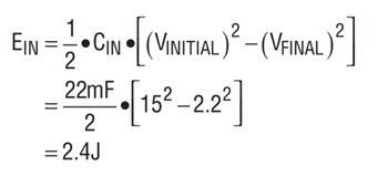
In this circuit, a stack of supercapacitors totaling 22mF is charged to 15V while the primary power source is active. A lower ESR electrolytic or ceramic cap is placed in parallel to minimize VIN ripple. The VCC supply pin is back-driven from the 5V output in this example, allowing the LTC3112’s gate drive circuits to operate efficiently with an input voltage from 15V down to 2.2V. Available energy at the input is given by:

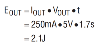
The results of the backup event are shown in Figure 7. A resistive network from VIN, VOUT and GND is used to drive the RUN pin to provide a clean shutdown of VOUT. In this example, a constant 250mA load is drawn from the LTC3112 resulting in the VIN capacitors maintaining regulation for 1.7 seconds, and an average conversion efficiency of 88% including the supercapacitor losses.


Figure 7. Supercap discharge performance during power supply backup event.
The prior example can be easily scaled depending on the voltage rating of the supercapacitors and the energy required for backup. The IOUT pin (Figure 6) can be monitored by an ADC to measure load current during the backup event. An important consideration in design is the maximum output current capability of the buck-boost converter. As shown in Figure 8, the LTC3112 is able to support up to 4A of load current when VIN >> VOUT. As the converter transitions from buck to boost mode, the maximum load current drops accordingly.

Figure 8. Maximum output current versus VIN with VOUT = 5V and VCC back-fed.
Summary
The LTC3112 produces low noise buck-boost conversion in a range of applications requiring an extended input or output voltage range. The LTC3112’s ability to support large load currents make it ideal for handheld devices with increased processing power. Solution size and conversion efficiency benefit from 50mΩ N-Channel MOSFET switches and thermally enhanced packages. To provide longer run times, a low Burst Mode quiescent current extends high efficiency over several decades of load current. Features such as synchronized switching frequency, programmable output voltage, a load current monitor and external loop compensation allow the LTC3112 to be tailored for a specific application.


