Minimizing Radiated Emissions From Multiple Power isoPower Devices in Dense PCB Layouts
iCoupler® digital isolators with integrated isolated power, isoPower,® employ isolated dc-to-dc converters that switch relatively large currents at frequencies in the 125 MHz to 200 MHz range. Operation at these high frequencies raises concerns about radiated emissions and conducted noise. Analog Devices AN-0971 Application Note, Recommendations for Control of Radiated Emissions with isoPower Devices, contains circuit and layout guidance to minimize radiated emissions. Practical reductions in peak emissions of greater than 25 dB are demonstrated through circuit optimization (lower load current and supply voltage) and the use of cross barrier stitching capacitance implemented with interplane PCB capacitance.
But what happens if you have multiple isoPower devices in the design and your layout is very dense? Can you still achieve meaningful reductions in radiated emissions? This note aims to provide a few general guidelines to help in this case.
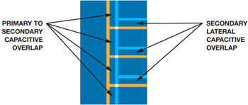
Interplane stitching capacitance is shown to provide the largest benefit, due to the low inductance structures that can be built. In a situation where overall PCB area is limited, multiple layers are your friend. Use as many layers as is practical, and overlap as many of the power and ground layers (reference layers) as possible. Figure 1 shows an example stackup.

Figure 1. Example PCB layer stackup.
Buried layers (3 and 4 on the primary side, 2 through 5 on the secondary side) carry the power and ground currents. Overlap across the barrier (for example between Layer 4, GND, on the primary side and Layer 3, V Iso, on the secondary side) creates the desired stitching capacitance. Multiple overlaps can be created with multilayer PCB stackups, increasing the total capacitance. It’s also important to reduce the thickness of the PCB dielectric material between the reference planes to maximize capacitance.
Another layout trick is to overlap the planes from adjacent isoPower channels. Figure 2 illustrates an example with four adjacent channels.

Figure 2. Four adjacent channels with overlapped stitching capacitance.
In this example each output domain is isolated from the others, but we can still take advantage of some overlap capacitance. Figure 3 shows the stackup, illustrating the increased capacitance that each isoPower device sees as well as linking adjacent isolated zones.

Figure 3. Four adjacent channels with overlapped stitching capacitance.
You must ensure that external and internal clearance requirements are met based on the end application. It can also be helpful to provide filtering on any cable connections using ferrite beads, to reduce antenna effects that may radiate.
In summary:
- Minimize power requirements for each channel
- Create stitching on multiple PCB layers
- Use as many PCB layers as is practical
- Use the thinnest dielectric possible between reference planes
- Couple between adjacent domains
- Ensure that internal and external creepage requirements are still met
- Provide filtering on any cable connections


