Clever Circuit Improves Efficiency of Charge Pump Plus Linear Regulator Solution
Clever Circuit Improves Efficiency of Charge Pump Plus Linear Regulator Solution
Oct 4 2016
In some systems, a charge pump plus linear regulator combination is preferred over an inductor-based switching power supply (with or without a post-regulating linear regulator) for several reasons: design simplicity, less radiated EMI, inductor-phobia, etc. For these applications, Analog Devices has a growing number of charge pump with integrated linear regulator solutions that provide a low output voltage noise alternative.
When efficiency is a concern, a charge pump has a fairly limited combination of output voltages it can provide. Charge pumps are great for doubling or inverting the input voltage. They also are good at providing half the input voltage. Figure 1a and 1b below show the two phases of the charge pump circuit (charge pump switch positions and current flow) when half the input voltage is desired at the output. The location of switches S2 and S4 have been exchanged to simplify drawing the circuit.

Figure 1a. 1/2 VIN Charge Pump, First Switch Phase
Note the flying capacitor and the output capacitor are placed in series during the first phase of the charge pump cycle, and then placed in parallel on the second phase to obtain half the input voltage. This circuit works for both positive and negative input voltages, i.e. if the input is positive then the output is half the positive input, and if the input is negative the output is half the negative input. But what if the only input voltage available is positive and a negative voltage at half the input voltage is desired? This is sometimes the case for designs where higher efficiency is a priority. For instance, what if the input voltage is 5V and a low noise –1.8V is needed? Using a simple charge pump plus linear regulator results in a solution that is very inefficient; the 5V is inverted to –5V at approximately 80% efficiency (the assumed charge pump efficiency) and then this is linear regulated down to –1.8V. The linear regulator efficiency is a very low (VOUT/–VIN = 36%) and when combined with the charge pump efficiency, gives a cascaded efficiency of only 29%. If the charge pump could provide –2.5V instead, the linear regulator efficiency would increase to 72% (–1.8V/–2.5V), thereby doubling the cascaded efficiency. Keep in mind the linear regulator must have a very low dropout (in this case less than –200mV) to provide the –1.8V regulated output voltage at the desired current level.
A circuit that provides –2.5V from the 5V input would be ideal, but as mentioned, this only works when the input and output are the same polarity. The problem arises because to invert the input voltage, both the flying capacitor and the output capacitor need to be floating at the same and then put in parallel, but there doesn't seem to be a way to do this based on the charge pump circuit diagram above.
A clever LTC3260 circuit shown in figure 2 provides a solution to the dilemma. Using external Schottky diode switches, the circuit produces a negative output voltage that is approximately half the input (minus the voltage drop across a Schottky diode), but of opposite polarity, yielding lower power dissipation on the negative supply.
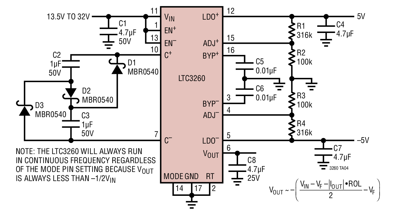
Figure 2. Efficient Inverting Low Noise Solution
The LTC3260 is a single input voltage, bipolar output, inductorless, low output voltage noise power supply that includes an inverting charge pump plus two linear regulators to provide a small footprint positive and negative output power supply. The device takes a positive input voltage between 4.5V to 32V and uses a 50mA low noise linear regulator with 800mV maximum dropout (at room temperature) to generate the positive output. It uses the charge-pump to invert the input voltage; this negative output voltage is also followed by a 50mA low noise linear regulator. The combination provides a simple, bipolar power supply with approximately 100µVRMS output noise and output voltages down to ±1.2V.
The circuit works as follows:
When switches S1 and S2 close (S3 and S4 are open), the two series capacitors are charged up to approximately half the input voltage ((VIN – VC1 –VC2 – VF) = 0V, where VF is the forward drop of the Schottky diode. Since the two capacitors are the same size, VC1 = VC2 = VC, the equation reduces to VIN = 2VC – VF.
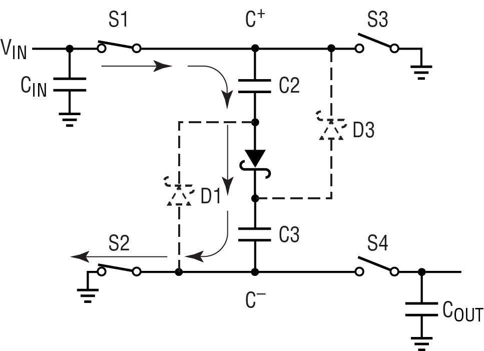
Figure 3. First Phase of ~1/2 Inverting Charge Pump
When S3 and S4 close (S1 and S2 are open), C+ is at ground (figure 4). Since the voltage across a capacitor cannot change instantaneously, the voltage at C– will be –VC + VF. The output effectively sees the D1 diode drop and C2 series combination in parallel with the series combination of C3 and D3. If the diodes were not used, the circuit would simply regulate to –VIN instead of ~1/2VIN.
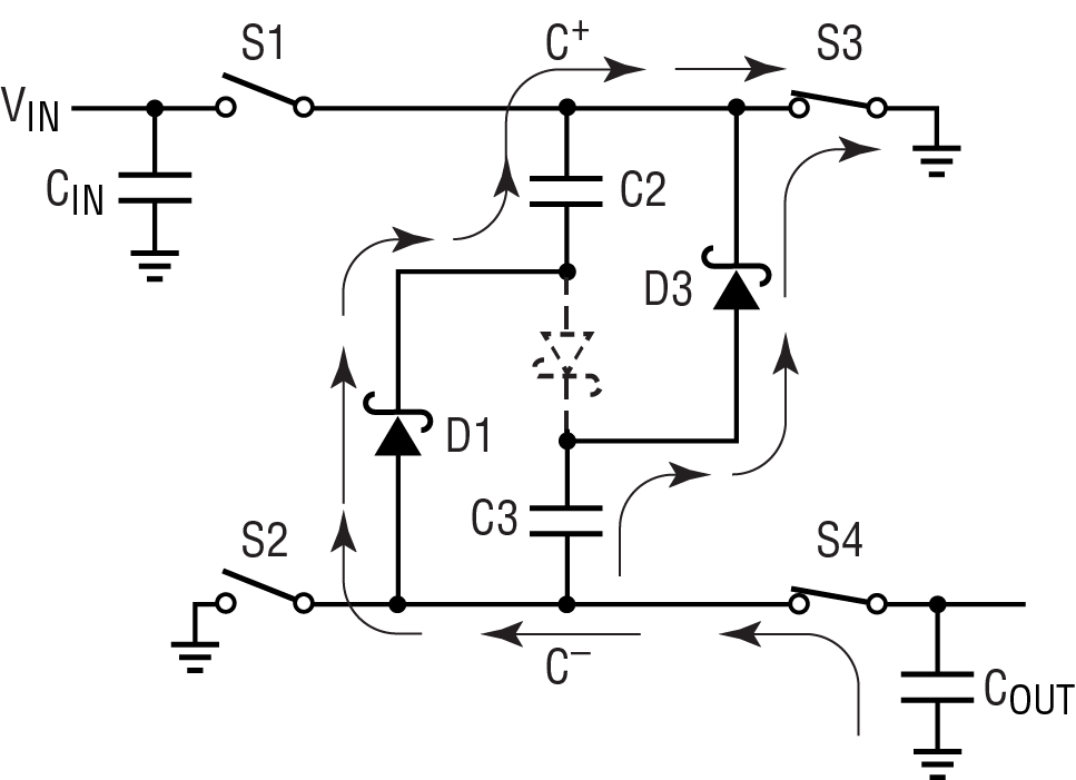
Figure 4. Second Phase of ~1/2 Inverting Charge Pump
Looking at a more extreme case of a 15V input voltage and a desired output of ±5V @ 50mA output, and again assuming the charge pump is 80% efficient, the two following scenarios are:
Case 1. Standard Inverting Charge Pump
- Positive Supply: 15V linear regulated to 5V = 33% efficient
- Negative Supply: 15V inverted with 80% efficiency and linear regulated to –5V = 26.4% efficient (0.8*–5V/–15V).
Case 2. Divide-By-2 Inverting Charge Pump Circuit
- Positive Supply: 15V linear regulated to 5V = 33% efficient
- Negative Supply: 15V inverted and divided by 2; VOUT = 6.25V.
In Case 2, the charge pump is slightly less efficient due to the Schottky diodes, but the linear regulator efficiency increases to approximately 80%, greatly increasing overall efficiency.
The LTC3260 is available in a space-saving 4mm × 3mm DFN-16 package in addition to the exposed pad MSOP-16 package (4.9mm × 4mm footprint). Other Analog Devices charge pump plus linear regulator solutions include the LTC3265 (a low noise dual supply solution with boost and inverting charge pumps and low noise ±50mA linear post-regulators) and the LTC3256 (a 38V input voltage, step-down charge pump converter with a 350mA charge pump followed by a 250mA low noise linear regulator). All of these solutions provide a low EMI, low noise, integrated power solution for applications where an inductor-based solution is not preferred. And as shown by the LTC3260 circuit, efficiency can be much higher than one might think possible with this creative circuit design technique.
About the Authors
Kevin Scott works as a Product Marketing Manager for the Power Products Group at Analog Devices, where he manages Boost, Buck-Boost and Isolated Converters, LED Drivers and Linear Regulators. He previously worked as a
Related to this Article
Products
Product Categories
Resources
Data Sheet
Product Selector Card


