Battery Stack Monitor Extends Life of Li-Ion Batteries in Hybrid Electric Vehicles
Battery Stack Monitor Extends Life of Li-Ion Batteries in Hybrid Electric Vehicles
by
Jon Munson
Mar 1 2009
Introduction
The cost of running a car on electricity is equivalent to paying $0.75/gallon for gasoline, and if that electricity comes from carbon neutral sources, car owners are saving both money and the environment (gasoline combustion produces 9kg of CO2 per US gallon). Advancements in battery technology (see sidebar), especially with Lithium-based chemistries, hold the greatest promise for converting the worldwide fleet of cars to hybrid or fully electric.
Lithium battery packs offer the highest energy density of any current battery technology, but high performance is not guaranteed simply by design. In real world use, a battery management system (BMS) makes a significant difference in the performance and lifetime of Li-Ion batteries—arguably more so than the design of the battery itself. The LTC6802 multicell battery stack monitor is central to any BMS for the large battery stacks common in electric vehicles (EVs) and hybrid electric vehicles (HEVs). Its robust design and high accuracy helps guarantee the performance and lifetime of expensive battery packs.
For instance, to meet a 15-year, 5000 charge cycle goal, only a portion (say 40%) of the battery pack’s cell-capacity can be used. Of course, using only 40% of the capacity essentially lowers the energy density of the pack. This is the problem: increasing battery lifetime is traded against the need to use as few kg of batteries as possible—the most expensive component in any EV. Only a well-designed BMS can maximize battery performance and lifetime in the face 200A peak charge and discharge currents.
Li-ion Batteries in Electric Vehicles and Hybrids
So why aren’t all cars electric? One reason is energy density. Gasoline holds 80 times the energy per kg as Li-ion batteries (Table 1) and refuels in three minutes, essentially allowing indefinite driving. Even a big lithium pack only gives a passenger car about a 100-miles after an 8-hour charging cycle. To drive a passenger car further than 100 miles you still need a gasoline engine, but even so, batteries improve gas mileage in hybrid electric vehicles (HEVs). The peak efficiency of the Otto cycle engine is only 30% at high RPMs and the average efficiency is about 12%. Using batteries to supply torque during acceleration and recover joules during regenerative braking means the gas engine runs less often and runs at a higher efficiency, effectively doubling the mpg.
| Medium | Wh/kg |
| Diesel Fuel | 12,700 |
| Gasoline | 12,700 |
| Li-Ion Battery | 150 |
| NiMh Battery | 100 |
| Lead Acid Battery | 25 |
In the 1970s the only available high power battery chemistry was lead acid, too heavy to reasonably power anything larger than a golf cart. Then came NiMh batteries, which improved energy density enough to enable the first commercially successful HEVs, like the Toyota Prius and Ford Escape. Li-ion batteries take energy density another step forward, by offering another 50% improvement. The safety of Li-ion was a concern, but new battery technologies like the A123 nanophosphate cell, the EnerDel Spinel-Titanate chemistry, the GS Yuasa EH6 design and others are as safe as NiMh, offer extremely high power (200A peak discharge rates), and last 10 to 15 years with proper charge management. By model year 2012, the majority of hybrid cars and trucks will use lithium battery technology.
Figure 1 shows a shows a block diagram of the battery pack with a BMS, and Figure 2 shows a typical HEV power train. The battery pack building block is a 2.5V to 3.9V, 4Ahr to 40Ahr Li-ion cell. 100 to 200 cells are connected in series to bring the battery pack voltage into the hundreds of volts. This DC power source drives a 30kW to 70kW electric motor. The pack voltage is high so that the average current is low for a given power level. Lower current reduces I2R power losses, so cables can be smaller, thus reducing weight and cost. The pack should be able to deliver 200A under peak conditions and be quickly rechargeable. In other words, the battery needs to offer high energy density and high power density, specifications that can be met by Li-ion batteries. Systems for busses and tractor-trailers use up to four parallel packs of 640V each.

Figure 1. 96-cell battery pack.


Figure 2 . Toyota Prius “split power” hybrid drive train.
Battery Management System Optimizes Li-Ion Run Time and Lifetime
In any battery stack, the more accurately you know state of charge (SOC) of each cell, the more cell capacity you can use while still maximizing cell life. In a laptop computer, gas gauging comes from monitoring cell voltage and counting coulombs in and out of the stack of four to eight cells. Voltage, current, time and temperature are combined in a robust algorithm to give an indication of the SOC. Unfortunately, it’s nearly impossible to count coulombs in a car. The battery drives an electric motor, not a motherboard, so it must handle current spikes of 200A, followed by low level idling. Furthermore, you have from 96 to 200 cells in series, in groups of 10 or 12. The cells age at different rates, were manufactured from multiple lots, and vary in temperature. Their capacities diverge constantly. Different cells with the same coulomb count can have wildly different charge levels.
That’s why the BMS focuses on cell voltage. If you can accurately measure the voltage of every cell, you can know the cell’s SOC with reasonable accuracy (Figure 3). The trick is to improve the accuracy of the voltage measurement by taking into account temperature effects on battery ESR and capacity. By constantly measuring each cell’s voltage, you keep a running estimation of each cell’s charge level. If some cells are overcharged and some under, they can be balanced by bleeding off charge (passive balancing) or redistributing charge (active balancing).

Figure 3. State of charge vs current and temperature for a typical Li-ion cell.
Accurate Monitoring is Key to Raising Battery Performance while Lowering Costs
The LTC6802 (Figure 4) is a precision data acquisition IC optimized for measuring the voltage of every cell in a large string series-connected batteries. In the BMS, the LTC6802 does the heavy lifting analog function, passing digital voltage and temperature measurements to the host processor for SOC computation. The LTC6802’s high accuracy, excellent noise rejection, high voltage tolerance, and extensive self-diagnostics make it robust and easy-to-use. The high level of integration means a substantial cost savings for customers when compared to discrete component data acquisition designs.

Figure 4. Simplified block diagram of the LTC6802.
Increasing measurement accuracy reduces battery cost, as illustrated by the following example. Figure 5 shows the typical performance of the LTC6802, where 0.1% total error from –20°C to 60°C translates to 4mV precision for a 3.7V cell. Suppose that to achieve a 15-year battery lifetime, you are limited to 40% of a cell’s capacity per charge cycle, and assume the cell voltage vs charge level of the battery is very flat, e.g., 1.25mV/%SOC. A measurement error of 4mV means the estimation of SOC is accurate to 3%. The BMS must charge cells to no more than 37% (40% – 3%) of their capacity to guarantee the 15-year lifetime.

Figure 5. Typical measurement accuracy vs temperature of seven samples.
Now consider a monitor IC with 10mV error over similar conditions. In this case, the BMS can only use 32% (40% – 10mV • 1%/1.25mV) of the cells’ capacity and still guarantee a 15-year life. This seemingly negligible increase in measurement error results in a significant 14% reduction in the usable capacity. That is, a vehicle requires least 14% more batteries, or at least 14% more weight, cost and electronics to travel an equivalent distance as a vehicle with the more accurate BMS. Batteries are expensive. It takes about $4000 worth of batteries to drive 50 miles, so the increased measurement error means $560 in additional cells. This is why BMS designers scrutinize every 0.01% of measurement error. Figure 6 shows a simple battery cost model as a function of BMS accuracy.

Figure 6. High BMS accuracy is important to keeping battery costs in check, as shown in this cost vs measurement error model.
Adding a low drift reference, an initial factory calibration, and a periodic self-calibration routine can improve the measurement accuracy of the LTC6802 to 0.03%. For example, in Figure 7 the LT1461A-4 is periodically applied to channel C1. The temperature stable LT1461 measurement is used to correct temperature drift in the LTC6802. The initial error of the LTC6802 and LT1461A is corrected by measuring and storing a calibration reference after board assembly.

Figure 7. Improving accuracy with calibration.
Inverter noise can seriously interfere with cell voltage measurements. When a 100-cell stack is loaded by an electric motor it can have a 370V open circuit voltage and up to 100V switching transients (Figure 8). Spreading the transient equally over the 100 cells means the top cell has 370V of common mode voltage, 100V of common mode transients, 1V of differential transients and an average DC value of 3.7V, which we need to measure to 4mV. Breaking the battery stack into 12-cell modules further reduces the common mode voltage. In a pack like Figure 2, each LTC6802 (one per module) sees up to 12V common mode transients and 1V differential transients per cell. The transients are at the PWM frequency of 10kHz to 20kHz. The LTC6802 has excellent common mode rejection (Figure 9) to eliminate this error term. The SINC2 filter inherent in the delta-sigma ADC attenuates the differential noise by 40dB (Figure 10). External filtering or measurement averaging can be used to further reduce the differential noise.

Figure 8. Inverter noise example.

Figure 9. Cell measurement common mode rejection.

Figure 10. Cell measurement filtering.
Diagnostic Features of the LTC6802 Improve Robustness
Automotive systems require that “no bad cell reading be misinterpreted as a good cell reading.” Two of the more common faults that can cause false readings are open circuits and IC failures. If there is an open circuit in the wiring harness and if there is a filter capacitor on the ADC input (Figure 11), the capacitor will tend to hold the input voltage at a point midway between the adjacent cells. Some type of open wire detection or cell resistance measuring function is necessary. The LTC6802 includes 100μA current sources to load the cell inputs. The current source will cause large changes in cell readings if there is an open circuit in the harness.
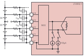
Figure 11. Current sources help detect open circuits.
The host controller must be able to run diagnostics on all the modules during normal operation to detect IC failures. If these periodic self-tests fail, then the control algorithm is suspect and the battery pack must be taken off line. The LTC6802 includes a built-in self-test in combination with external support circuits to allow the BMS to completely verify the data acquisition system. See the LTC6802 data sheets for more details.
The LTC6802 Isolates Communications from Swings in Ground Potential
Breaking a ~100 cell pack into modules makes it easier to integrate the analog circuits. Unfortunately, we are left with the task of getting the data from measurement IC to the host controller when the difference in ground potential exceeds 300V. The LTC6802 can solve this problem in a number of ways, depending on the specific needs of the application.
The LTC6802 comes in two flavors, depending on the desired data communication scheme. The LTC6802-1 offers a built-in stackable serial peripheral interface (SPI) solution designed for easy daisy chaining of the interface. The addressable LTC6802-2 is designed for bus-oriented (parallel) SPI communication, but it can also be used in a parallel-addressable, daisy chained interface for a robust and relatively inexpensive solution. All three schemes are described below.
SPI Bus Communication with the Addressable LTC6802-2 and Digital Isolators
The most straightforward approach is to use a bus communications scheme, with a digital isolator between each module and the host controller. Figure 12 shows a 96-cell pack using eight multicell modules monitored by the LTC6802. The physical layer is a 4-wire SPI bus. An addressing scheme allows the control module to talk to the battery modules separately or in unison. The data buses on the modules are isolated from one another. This is a robust scheme, but it has one major drawback: digital isolators are expensive and require an isolated power supply so that the battery cells don’t have to provide the power to the cell side of the isolator.

Figure 12. Using digital isolators to communicate to the LTC6802.
Daisy Chaining the SPI Interface with the LTC6802-1
The LTC6802-1 provides fixed 1mA signaling between stacked devices to enable easy implementation a daisy chained SPI interface with inexpensive support circuitry. The digital isolators are eliminated as shown in Figure 13. The interface exploits the fact that the positive supply of module “N” is the same voltage as the ground of module “N+1.” A 1mA current is used to transmit data between adjacent modules. Like the analog circuits, the modular approach means the data bus has to deal with a fraction of the total pack voltage.

Figure 13. Using the daisy chained SPI to eliminate digital isolators.
The disadvantage of any pure daisy chain is that a fault in one module results in a loss of communications with all the modules above it in the stack. Also, since there is no galvanic isolation between modules, the interface needs to handle large voltages that occur during fault conditions. For example if the “service switch” in Figure 1 is open and there is a load on the pack then the data bus connection between modules 4 and 5 will see a reverse voltage equal to the total pack voltage (–300V to –400V). The LTC6802 interface relies on external discrete diodes to block the reverse voltage during fault conditions.
The Best of Both Worlds: Daisy Chained, Addressable Interface with the LTC6802-2
With inexpensive external circuitry, the LTC6802-2 can also be used in a stacked SPI configuration like the LTC6802-1, but with more flexibility in the operating parameters.
The SPI port of the LTC6802-2 is a 4-wire connection: chip select in (CSBI), clock in (SCKI), data in (SDI), and data out (SDO). The inputs are conventional CMOS levels and the output is an open-drain NMOS. The SDO pin must have an external pull-up current or added resistance suitable for the intended data rate. The IC also provides a versatile always-on 5V output (VREG), which can produce up to 4mA to energize low power auxiliary circuitry.
Figure 14 shows a complete stacked LTC6802-2 SPI interface for a 36-cell application. The stack can be increased in size by replicating the circuit of the middle IC. In Figure 14, the VREG and V– pins of each stacked IC are used to bias common-base connected transistors to form a signal translation current for each SPI data line. Each LTC6802 can monitor up to 12 cell-potentials, which could sum to 60V in certain instances, so the transistors selected for the SPI translation need to have a VCBO over 60V, but they should be the highest available fT to prevent undue slowing of the logic signals. A suitable NPN candidate is the CMPT8099, while the CMPT8599 is its PNP complement, both from Central Semiconductor. These are fast 80V devices (fT > 150MHz).

Figure 14. Inexpensive SPI daisy chain for parallel-addressed LTC6802-2.
Sending Signals Upwards
At the bottom-of-stack IC, the logic signal is furnished by the host connection, be it a microprocessor or an SPI isolation device. By simply pulling down the emitter leg of an NPN having a VREG base potential through a known resistance, a specific current is formed for a logic low input signal. In the case of the component values shown, the current is about 2mA for a logic low, and conversely, the transistor is essentially turned off with a logic high (~0mA for 5V logic).
Since the collector current is nearly identical to the emitter current, the same current pulls on the next higher cascode circuit. Since that next circuit is the same as the first, the voltage on the upper emitter resistor reproduces that of the bottom circuit logic level for the upper IC. This continues up the daisy chain, eventually terminating at the top potential of the battery stack. Since each IC is provided the same input waveforms, this structure forms a parallel bus from a logical perspective, even though each IC is operating at a different potential in the stack.
The NPN transistors at the top IC source the logic current directly from the battery stack. Only small base currents flow from any VREG output. The 600V collector diodes provide reverse-voltage protection in the event a battery group interconnection is lost, perhaps during service (these are not required for functionality and could be omitted in some situations).
Bringing Data Down the Stack
The SDO cascode chain is similar in concept, except the current starts at the top of the stack and flows downward. At the top IC, a PNP transistor with its base connected to the local V– pin has current injected into its emitter by a pullup resistor. Here again, the collector current is essentially identical to the emitter current, and so current flows downward through each successive PNP and terminates into a resistor at the bottom of stack. In this case, the presence of the current in the termination resistor, about 2mA for the component values shown, forms a logic high potential for the host interface.
A Schottky diode is connected from each SDO pin to the emitter of a local PNP thereby allowing any LTC6802 on the stack to divert the pullup current to the local V– when outputting a logic low. This effectively turns off the emitter current to the local PNP transistor and all points lower in the stack, so the voltage on the bottom termination resistor then drops to a logic low level. Since each SDO pin can force a low level, this forms a wire-OR function that is equivalent to paralleled connections as far as the host interface is concerned. Note the bottom of stack SDO diode is connected slightly differently; it forms a direct wire-OR at the host interface. Since the LTC6802-2 is designed to use addressed readback commands, this line is properly multiplexed and no inter-IC contention occurs.
To eliminate the pull-up current during standby, a general purpose N-channel MOSFET is used to interrupt the top PNP emitter current when the watchdog timer bit goes low. The watchdog timeout will release when clock activity is present, so the SDO line will reactivate as needed. Here again, an NPN is used at the top of stack to ensure the pull-up current comes directly from the battery, rather than loading VREG.
Collector diodes are added here as well to provide a high reverse voltage protection capability, plus some added series resistance is included to protect the lower transistor emitters from transient energy (once again, these protection parts don’t add any other functionality to the data transmission and could be omitted in some circumstances).
External SPI Advantages
Since the LTC6802-2 uses a parallel addressable SPI protocol, the conventional method of connecting multiple devices in a stack is to provide isolation for each SPI connection, then parallel the signals on the host side. Isolators are relatively expensive and often need extra power circuitry, thus adding significantly to the total solution cost. The transistor circuitry shown here is quite inexpensive and offers the option to make certain design tradeoffs as well. With the propagation delays involved and desire to keep power fairly low, this circuit as shown still communicates at over 500kbps. Lower SPI currents could be chosen in applications that don’t demand the high data rate by simply raising the resistance values accordingly.
The main feature of the transistorized SPI bus is the wide compliance range that is afforded by the unconstrained collector -base operating range of the transistors. In normal operation the VCB ranges from just less than the cells connected to the LTC6802, to some five volts below that, depending on the logic level transmitted. This becomes important since voltage fluctuations on the battery, due to load dynamics or switching transients, affect the VCB of the transistors even though the V+ and ADC cell inputs may be filtered. Some vehicle manufacturers are requiring that a BMS tolerate 1V steps with 200ns rise/fall time per cell in the stack, so this is a 12V waveform edge as seen by the transistors in a typical application. With the low collector capacitance and 2mA logic level of the transistor chain, SPI transmissions remain error free with even this high level of noise.
Conclusion
EVs and HEVs are here to stay. Inherently safe lithium batteries, which combine energy density, power density, and cycle life, will continue to evolve to improve the performance of these vehicles. Battery management systems using the LTC6802 extract the most driving distance and lifetime from the battery pack while lowering system cost.
About the Authors
Jon Munson is a senior applications engineer for Analog Devices, supporting their Signal Conditioning product line. Jon has a BS in electrical engineering and computer science from Santa Clara University. He has designed h...
Related to this Article
Products
NOT RECOMMENDED FOR NEW DESIGNS
12 Channel Multicell Battery Monitor with Daisy Chain Interface, Generation 1
NOT RECOMMENDED FOR NEW DESIGNS
12 Channel Multicell Battery Monitor with Addressable Interface, Generaion 1
PRODUCTION
Micropower Precision Low Dropout Series Voltage Reference Family