


Overview
Design Resources
Design & Integration File
- Schematic
- Bill of Materials
- Gerber Files
- PADS Files
- Assembly Drawing
Evaluation Hardware
Part Numbers with "Z" indicate RoHS Compliance. Boards checked are needed to evaluate this circuit.
- EVAL-CFTL-6V-PWRZ ($23.01) Wall Power Supply for Eval Board
- EVAL-CN0272-SDPZ ($135.36) 2 MHz Bandwidth PIN Photodiode Preamp with Dark Current Compensation
- EVAL-SDP-CB1Z ($134.00) Eval Control Board
Features & Benefits
- High speed photodiode signal conditioning circuit
- 91dB dynamic range and circuit consumes only 40 mA
- Dark current compensation
- Spectral range from 400 nm to 1050 nm
- Well suited for portable high speed applications
Markets and Technologies
Parts Used
Documentation & Resources
-
CN-0272 Software User Guide10/22/2018WIKI
-
CN-0272: 2 MHz Bandwidth PIN Photodiode Preamp with Dark Current Compensation4/10/2013PDF376 kB
Circuit Function & Benefits
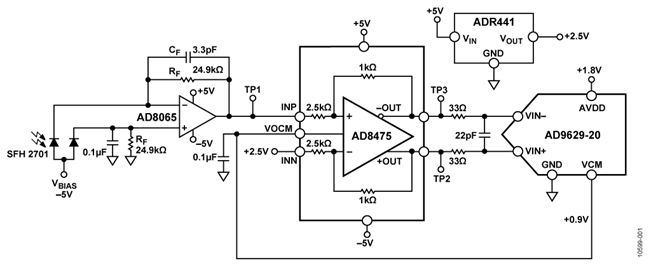
The circuit shown in Figure 1 is a high speed photodiode signal conditioning circuit with dark current compensation. The system converts current from a high speed silicon PIN photodiode and drives the inputs of a 20 MSPS analog-to-digital converter (ADC). This combination of parts offers spectral sensitivity from 400 nm to 1050 nm with 49 nA of photocurrent sensitivity, a dynamic range of 91 dB, and a bandwidth of 2 MHz. The signal conditioning circuitry of the system consumes only 40 mA of current from the ±5 V supplies making this configuration suitable for portable high speed, high resolution light intensity applications, such as pulse oximetry.


Other suitable applications for this circuit are as an analog opto-isolator. It can also be adapted to applications that require larger bandwidth and less resolution such as adaptive speed control systems.
This circuit note discusses the design steps needed to optimize the circuit shown in Figure 1 for a specific bandwidth including stability calculations, noise analysis, and component selection considerations.
Circuit Description
Component Selection
Photodiodes are high impedance sensors used to detect the intensity of light. Photodiodes do not have internal gain but can operate at much higher light levels than other light detectors.
Photodiodes operate either with zero bias (photovoltaic mode) or with a reverse bias (photoconductive mode). The most precise linear operation is obtained in the photovoltaic mode, while higher switching speeds are realizable when the diode is operated in the photoconductive mode at the expense of linearity. Under these reverse bias conditions, a small amount of current called dark current flows even when there is no illumination. The dark current error can be cancelled using a second photodiode of the same type in the noninverting input of the op amp as is shown in Figure 1.
Three factors influence the response time of a photodiode
- The charge collection time of the carriers in the depleted region of the photodiode
- The charge collection time of the carriers in the undepleted region of the photodiode
- The RC time constant of the diode circuit combination
Because the junction capacitance is dependent on the diffused area of the photodiode and the applied reverse bias, faster rise times are obtained with smaller diffused area photodiodes and larger applied reverse biases. The junction capacitance for the SFH 2701 PIN photodiode used in the CN-0272 circuit note is 3 pF typical, 5 pF maximum for 0 V bias. The typical capacitance is 2 pF for 1 V reverse bias and 1.7 pF for 5 V reverse bias. Measurements in the circuit were all taken with a reverse bias of 5 V.


Figure 2 shows an I/V converter with an electrical model of a photodiode. The basic transfer function is

Where IPHOTO is the output current of the photodiode, and the parallel combination of RF and CF sets the signal bandwidth. Ideally, all of the output current from the photodiode passes through RF, but all op amps have input bias currents that introduce errors on the output. Op amps with picoamps of input bias current and low input offset voltages are preferred to minimize the error. The AD8065 has only 2 pA of input bias current and only 400 μV of input offset voltage.
The circuit is designed to have a full scale output of 5 V with a maximum photodiode current of 200 μA. This determines the value of the feedback resistor to be

The stable bandwidth attainable with this preamp is a function of RF, the gain bandwidth product of the amplifier (65 MHz), and the total capacitance at the amplifier’s summing junction, CIN. For this circuit, the SFH 2701 diode (OSRAM Opto Semiconductors GmbH) has a maximum capacitance of CD = 5 pF. The AD8065 common-mode input capacitance is CM = 2.1 pF, and the differential-mode input capacitance is CD = 4.5 pF. Therefore, the total input capacitance is CIN = 11.6 pF.
It can be shown that the signal bandwidth resulting in a 45° phase margin, f(45), is defined by

Because the maximum attainable bandwidth is larger than the intended bandwidth, the AD8065 is a good candidate for the application, which is largely due to its large ratio of fCR to CIN.
RF and CIN produce a pole in the loop transfer function of the amplifier that can result in peaking and instability (see Figure 3). Adding CF creates a zero in the loop transfer function that compensates for the effect of the pole and reduces the signal bandwidth.


The value of CF that produces 2 MHz of bandwidth with the selected value of RF is

To determine if 3.3 pF is enough capacitance to stabilize the system, calculate the amount of capacitance needed to obtain 45° of phase margin. The value of CF that produces f(45) can be shown as

Because the intended value of 3.3 pF is larger than the minimum value of 1.1 pF, the system is stable because increasing the capacitance increases the amount of phase margin.
Noise Analysis
Now that the components are selected, how much resolution is needed to convert the signal must be determined. As in most noise analyses, only the key contributors need to be identified. Noise sources combine in an RSS manner; therefore, any single noise source that is at least three-to-four times larger than any of the others dominates.
In the case of the photodiode preamp, the dominant sources of output noise are the input voltage noise of the op amp and the feedback resistor noise. The input current noise of the FET-input op amp is negligible. The shot noise of the photodiode (caused by reverse bias) is negligible because of the filtering effect of the shunt capacitance.
The resistor noise is calculated using the Johnson noise formula.

where:
k is Boltzmann’s constant (1.38 × 10⁻²³J/K).
T is the absolute temperature in Kelvin.
The factor of 1.57 converts the approximate single-pole bandwidth into the equivalent noise bandwidth.
Note that the 0.1 μF capacitor on the positive input of the preamp eliminates the high frequency noise produced by the second RF resistor used to cancel the effects of bias current.
The primary source of output noise is due to the input voltage noise and the high frequency noise gain peaking that occurs between f1 and fCR. If it is assumed that the output noise is constant over the entire range of frequencies and the maximum value for the ac noise gain is used, then

where VN is the input voltage noise of the amplifier (7 nV/√Hz).
The total rms noise referred to the output is then the RSS value of the two components

The total output dynamic range of the preamp can be calculated by dividing the full scale output signal (5 V) by the total output rms noise (67 μV rms) and converting it to decibels, yielding approximately 97 dB.

ADC Selection
Because the amount of noise output by the amplifier is known the maximum number of bits that can be resolved can now be calculated by dividing the full scale output by the rms noise.

The number of rms LSBs can be converted into effective resolution.

Noise-free code resolution can be obtained by subtracting 2.7 bits from effective resolution.

Depending on the end application, 13 bits may be more resolution than is actually needed. Because the intended application does not require this amount of resolution, it has been confirmed that the system meets the design requirements with 12 bits.
If the LSB size (in current) is smaller than the amount of dark current, as mentioned earlier, the dark current can be canceled using a second photodiode of the same type in the noninverting input of the op amp. For example, if 16 bits of resolution is needed, the amount of photocurrent detected is

Since the maximum amount of dark current that flows in the SFH 2701 is specified at 5 nA, dark current compensation is needed in a 16-bit design.
This application uses a 12-bit ADC; therefore, the LSB size is 49 nA, and it does not require dark current compensation.
If the bandwidth is 2 MHz, a reasonable guideline is to select an ADC with a sampling rate 10 times greater or more. This means the ideal ADC must sample at a rate of 20 MSPS with 12 bits of resolution.
The AD9629-20 is a good candidate because it is a 20 MSPS ADC with 12 bits of resolution. However, it requires differential inputs, and the 5 V p-p single-ended signal must be converted to a 2 V p-p differential signal. This is easily accomplished by using the AD8475 differential funnel amplifier, which simplifies the single-ended-to-differential conversion, and provides common-mode level shifting and precision attenuation.
The AD8475 has only a 500 μV maximum output offset, a 10 nV/√Hz differential output noise, and −112 dB total harmonic distortion plus noise (THD + N).
The AD8475 can support a maximum output voltage of 2 V p-p up to 10 MHz, which is well within the design requirement of 2 MHz.
The gain of the AD8475 was determined by the analog input span of the AD9629-20 (2 V p-p) and the full scale output of the AD8065 (5 V p-p).

An on-chip, common-mode voltage of 0.9 V is included in the AD9629-20 and is available from the VCM pin. This pin drives the VOCM pin of the AD8475 with the common-mode voltage of 0.9 V.
It is important to include the noise contribution of the AD8475 in this system. This is calculated by first multiplying the output noise of the AD8065 (67 μV rms) by the gain of the AD8475 to get the contribution due to the AD8065.

The output noise due to the AD8475 is calculated by multiplying the output noise density (10nV/√Hz) by the square root of the bandwidth set by the output filter.


The total noise at the output of the AD8475 after the filter is calculated by taking the RSS value of the two components is

With the noise contribution of the AD8475 incorporated into the calculations, the number of bits that can be resolved can be confirmed, and the total dynamic range can be calculated.

Test Results
A laser diode was used to drive the D1 photodiode and generate a current. Photodiode D2 is used for dark current compensation and is covered with an optically opaque epoxy (EPO-TEK® 320) to prevent output current from D2 when D1 is excited.
By forcing the photodiode to drive a larger than expected current, the approximate maximum rise and fall time of the AD8065 was 72 ns (see Figure 4).


A more realistic rise and fall time of the system can be measured by moving the position of the laser diode so that it does not overdrive the photodiode current beyond 200 μA. Figure 5 shows the measured rise and fall time of the AD8065 to be 282 ns and 290 ns, respectively. It is important to note that there is no ringing after the laser diode has turned off in both test cases because there is sufficient phase margin.


Now that the response of the system to a pulse of bright light has been tested, how the system responds to high speed changes in light intensity can be tested. An Agilent 33250A function generator was used to drive a laser diode with a 2 MHz sine wave. Figure 6 shows that the output of the AD8065 was able to successfully detect the small changes in light intensity, and Figure 7 shows a screenshot of the CN0272 Evaluation Software successfully receiving conversion data from the AD9629-20 ADC and plotting the data in a chart.


A complete design support package for this circuit note can be found at http://www.analog.com/CN0272-DesignSupport.
Applications in Pulse Oximetry
A pulse oximeter is a medical device used for continuously measuring the percentage of hemoglobin (Hgb) saturated with oxygen and the pulse rate of a patient. Hemoglobin carrying oxygen (oxyhemoglobin) absorbs light in the infrared region (940 nm) of the spectrum; hemoglobin that is not carrying oxygen (deoxyhemoglobin) absorbs visible red light (650 nm). The percentage of oxygen in the body is determined by calculating the ratio between these two intensities of light.
In a pulse oximeter, two LEDs (one emitting red light and the other emitting infrared light) are rapidly and sequentially excited by two current sources and a photodiode is used to detect the intensity of the light from the LEDs. The circuit shown in Figure 1 can be synchronized with an LED current sink circuit, such as CN-0125, to capture the light from each LED as it transmits through the tissue.
Common Variations
The components selected were optimized for noise and cost; however, other combinations can be substituted.
Other suitable dual supply amplifiers are the ADA4817-1 and ADA4637-1. If single supply operation is required, the AD8605 or the AD8615 are suggested. These amplifiers all have less than 2 pA of input bias current, less than 400 μV of input offset, and more than 10 MHz of unity-gain bandwidth products.
For applications requiring 100 MHz of bandwidth or greater, such as adaptive speed control, the combination of the ADA4817-1 FastFET amplifier, the ADA4932-1 low power differential ADC driver, and the 12-bit, 210 MSPS AD9634-210 ADC are suggested.
The ADA4817-1 has a high gain bandwidth product of 400 MHz and extremely small input capacitance of 1.4 pF. This makes the amplifier ideal for wideband transimpedance applications.
The ADA4932-1 driver can maintain 2 V p-p outputs up to 360 MHz, which is sufficient for the AD9634-210 ADC.
Circuit Evaluation & Test
This circuit uses the EVAL-CN0272-SDPZ circuit board and the EVAL-SDP-CB1Z SDP-B System Demonstration Platform controller board. The two boards have 120-pin mating connectors, allowing for the quick setup and evaluation of the performance of the circuit. The EVAL-CN0272-SDPZ board contains the circuit to be evaluated, as described in this note, and the SDP-B controller board is used with the CN0272 Evaluation Software to capture the data from the EVAL-CN0272-SDPZ circuit board.
Equipment Needed
The following equipment is needed:
- A PC with a USB port and Windows® XP (32 bit), Windows Vista®, or Windows® 7
- The EVAL-CN0272-SDPZ circuit board
- The EVAL-SDP-CB1Z SDP-B controller board
- The CN0272 SDP Evaluation Software
- The EVAL-CFTL-6V-PWRZ dc power supply or equivalent 6 V/1 A bench supply
- A light source between 400 nm to 1050 nm
Getting Started
Load the evaluation software by placing the CN0272 evaluation software into the CD drive of the PC. Using My Computer, locate the drive that contains the evaluation software.
Functional Block Diagram
See Figure 1 for the circuit block diagram and the EVAL-CN0272- SDPZ-PADSSchematic-RevC.pdf file for the complete circuit schematic. This file is contained in the CN0272 Design Support Package.


Setup
Connect the 120-pin connector on the EVAL-CN0272-SDPZ circuit board to the CON A connector on the EVAL-SDP-CB1Z controller board (SDP-B). Use nylon hardware to firmly secure the two boards, using the holes provided at the ends of the 120-pin connectors. With power to the supply off, connect a 6 V power supply to the +6 V and GND pins on the board. If available, a 6 V wall wart can be connected to the barrel connector on the board and used in place of the 6 V power supply. Connect the USB cable supplied with the SDP-B board to the USB port on the PC. Do not connect the USB cable to the Mini-USB connector on the SDP-B board at this time.
Test
Apply power to the 6 V supply (or wall wart) connected to the EVAL-CN0272-SDPZ circuit board. Launch the evaluation software and connect the USB cable from the PC to the Mini-USB connector on the SDP-B board.
Once USB communications are established, the SDP-B board can be used to send, receive, and capture parallel data from the EVAL-CN0272-SDPZ board.
Figure 9 shows a photo of the EVAL-CN0272-SDPZ evaluation board connected to the SDP board. Information regarding the SDP-B board can be found in the EVAL-CN0272-SDPZ SDP-B User Guide.
Note that photodiode D2 is used for dark current compensation and is covered with an optically opaque epoxy (EPO-TEK 320) to prevent output current from D2 when D1 is excited.
Information and details regarding test setup and calibration, and how to use the evaluation software for data capture can be found in the CN-0272 Software User Guide: http://www.analog.com/CN0272.pdf.


Connectivity for Prototype Development
The EVAL-CN0272-SDPZ evaluation board is designed to use the EVAL-SDP-CB1Z SDP-B board; however, any microprocessor can be used to interface to the parallel peripheral interface (PPI) of the AD9629-20. In order for another controller to be used with the EVAL-CN0272-SDPZ evaluation board, software must be developed by a third party.
There are existing interposer boards that can be used to interface to the Altera and Xilinx field programmable gate arrays (FPGAs). The BeMicro SDK board from Altera can be used with the BeMicro SDK/SDP interposer using Nios Drivers. Any Xilinx evaluation board that features the FMC connector can be used with the FMC-SDP Interposer board.