Design Note 346: PCI Express Power and Mini Card Solutions
Introduction
PCI Express is the third generation of PCI (Peripheral Component Interconnect) technology used to connect I/O peripheral devices in computer systems. It is intended as a general purpose I/O device interconnect that meets the needs of a wide variety of computing platforms such as desktop, mobile, server and communications. It also specifies the electrical and mechanical attributes of the backplane, connectors and removable cards in these systems.
Power Requirements
Each add-in card connector requires two power rails: 12V and 3.3V, along with a third, optional 3.3V auxiliary rail. If the designer elects to provide the auxiliary 3.3V rail in his system or if the platform supports the WAKE# signal, the 3.3VAUX rail must be supplied to all connectors.
In PCI Express, as in PCI, the Hot Swap™ controller is resident on the platform side of the system, delivering power to the connectors only after a card is inserted. This way, empty and otherwise unused connectors are safely unpowered, reducing the risk of inadvertent power supply faults, connector damage and simplifying power-up when a card is inserted into the connector.
Table 1 shows the PCI Express power supply rail specifications per connector, based on the number of connectors in the system.
| POWER RAIL | ×1 CONNECTOR | ×4/×8 CONNECTOR | ×16 CONNECTOR |
| 12V Supply Current Capacitive Load | 0.5A 300μF | 2.1A 1000μF | 4.4A (Up to 5.5A) 2000μF |
| 3.3V Supply Current Capacitive Load | 3A 1000μF | 3A 1000μF | 3A 1000μF |
| 3.3VAUX Supply Current Capacitive Load |
0.375A 150μF | 0.375A 150μF | 0.375A 150μF |
PCI Express Mini Card also provides two power sources: 3.3V and 1.5V. The auxiliary voltage (3.3VAUX) is sourced over the same pins as the primary 3.3V supply and is available during the standby/suspend state to support wake-event processing on the Mini Card. Table 2 summarizes PCI Express Mini Card power specifications.
There is no requirement for supply sequencing in either PCI Express or PCI Express Mini Card; the supplies may come up or go down in any order.
| POWER RAIL | PRIMARY POWER |
AUXILIARY POWER | ||||
| 3.3V Peak Supply Current | 1A | — | ||||
| 1.5V Peak Supply Current | 0.5A | — | ||||
| 3.3VAUX Peak Supply Current | 0.33A | 0.25A | ||||
| Note: All values are maximums. | ||||||
Circuit Solutions
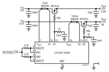
Figure 1 shows a circuit for a ×16 connector PCI Express system, implemented with an LTC1647 dual Hot Swap controller. As shown, port power is gated by a control signal applied through 4.7k resistors to the ON pins. The FAULT outputs are cross-coupled with the ON pins such that if an overcurrent fault occurs on either supply, the unaffected rail also shuts down. Shutdown is reset by toggling the control signal into the off state for at least 100μs.

Figure 1. PCI Express Port Power for ×16 Connector Satisfies dV/dt Specifications, Soft-Starts Full Load Capacitance and Guards Against Short Circuits and Overloads.
The supply rails slew at less than 1.5V/ms, well under any of the PCI Express limits. Thus the only alteration necessary to scale the design for ×1, ×4 and ×8 connector systems is to replace the 12V supply sense resistor with 70mΩ (×1) or 15mΩ (×4/×8) as appropriate.
Figure 2 shows a current limited circuit breaker for the optional 3.3VAUX rail, using the LTC4210 Hot Swap controller in a 6-lead ThinSOT™ package. With the ON pin (3) hard-wired to 3.3V, the LTC4210 operates autonomously, featuring a timed current limit to protect against overloads. Should the circuit breaker trip in the presence of a sustained fault, the LTC4210 automatically restarts after a time delay, requiring no intervention on the part of the PCI Express port manager.

Figure 2. Optional 3.3VAUX Port Power with Self Reseting, Current-Limited Circuit Breaker Operates Autonomously or Under Logic Control.
PCI Express Mini Card Mini
Card circuit requirements differ from PCI Express in several ways, but most importantly the Hot Swap controller resides on the card itself. In this configuration, it is important for the Hot Swap controller to monitor the incoming power and switch on only when those voltages are fully established.
Figure 3 shows a Mini Card Hot Swap control circuit implemented with an LTC1645, with undervoltage and overcurrent monitoring on both the 3.3V and 1.5V supplies. A fault on either supply rail causes both channels to shut down simultaneously. An open-drain signal at the ON pin permits optional logic control over the LTC1645. Similar to the LTC1647, pulsing ON low resets the LTC1645 after a fault.

Figure 3. PCI Express Mini Card. Hot Swap Circuit Resides on Mini Card.
For 3.3VAUX, simply add the circuit of Figure 2 in parallel at the 3.3V output. Note that with both circuits enabled and providing power to the 3.3V output, the available current is greater than 1.5A.
A complete definition of the PCI Express power delivery requirements is found in the PCI Express Card Electromechanical Specification and PCI Express Mini Card Electromechanical Specification. Further information is available at www.pcisig.com.
