AN-952: ADG9xx Wideband CMOS Switches: Frequently Asked Questions
Introduction
The ADG9xx CMOS wideband switches are designed primarily to meet the requirements of devices transmitting at industrial, scientific, and medical (ISM) band frequencies (≥900 MHz). The low insertion loss, high isolation between ports, low distortion, and low current consumption of these devices make them an excellent solution for many high frequency applications that require low power consumption and the ability to handle transmitted power (up to 16 dBm). Typical applications include high speed filtering and data routing.
Complete specifications for each part (ADG901, ADG902, ADG904, ADG904R, ADG918, ADG919, ADG936, and ADG936R) can be found in the data sheets available from Analog Devices, Inc., and should be consulted in conjunction with this application note. This application note addresses some of the frequently asked questions about these parts. A full list of ADG9xx parts is shown in Table 1.
| Part No. | Function1 | Power Supply | Insertion Loss @ 1 GHz (dB) | Isolation @ 1 GHz (dB) | Maximum Input Power, No DC Bias (dBm) | Maximum Input Power with 0.5 V DC Bias (dBm) | Package | ||
| ADG901 | 1 × SPST; Absorptive | 1.65 V to 2.75 V | −0.8 | −37 | 7 | 16 | 8-Lead MSOP and 8-Lead 3 mm × 3 mm LFCSP |
||
| ADG902 | 1 × SPST; Reflective | 1.65 V to 2.75 V | −0.8 | −37 | 7 | 16 | 8-Lead MSOP and 8-Lead 3 mm × 3 mm LFCSP |
||
| ADG918 | 1 × SPDT; Absorptive | 1.65 V to 2.75 V | −0.8 | −43 | 7 | 16 | 8-Lead MSOP and 8-Lead 3 mm × 3 mm LFCSP |
||
| ADG919 | 1 x SPDT; Reflective | 1.65 V to 2.75 V | −0.8 | −43 | 7 | 16 | 8-Lead MSOP and 8-Lead 3 mm × 3 mm LFCSP |
||
| ADG936 | 2 × SPDT; Absorptive | 1.65 V to 2.75 V | −0.9 | −36 | 7 | 16 | 20-Lead TSSOP; 20-Lead, 4 mm × 4 mm LFCSP |
||
| ADG936R | 2 × SPDT; Reflective | 1.65 V to 2.75 V | −0.9 | −36 | 7 | 16 | 20-Lead TSSOP; 20-Lead, 4 mm × 4 mm LFCSP |
||
| ADG904 | 4:1 Mux; Absorptive | 1.65 V to 2.75 V | −1.1 | −37 | 7 | 16 | 20-Lead TSSOP; 20-Lead, 4 mm × 4 mm LFCSP |
||
| ADG904R | 4 × SPDT; Reflective | 1.65 V to 2.75 V | −1.1 | −37 | 7 | 16 | 20-Lead TSSOP; 20-Lead, 4 mm × 4 mm LFCSP |
||
| 1 Absorptive (matched): switch with 50 Ω terminated shunts to ground. Reflective: switch with 0 Ω terminated shunts to ground. | |||||||||
Frequently Asked Questions
Supply Voltage
What is the voltage supply range for the ADG9xx products?
The ADG9xx are wideband switches using a CMOS process to provide high isolation and low insertion loss to 1 GHz. These parts can be operated from 1.65 V to 2.75 V and are fully characterized over this voltage range. The VDD supply should be fully decoupled to ground. The ADG9xx evaluation boards place two 10 μF surface-mount tantulum decoupling capacitors on the VDD line, with one placed close to the DUT along with a 100 pF ceramic capacitor on the VDD line.
For optimum performance, at what supply voltage should the part be operated?
A higher supply voltage on VDD generally gives better performance. Insertion loss performance is better with higher supplies as can be seen from plots in the individual data sheet. IP3 and P1dB are also slightly better with a higher supply voltage. Isolation performance does not vary significantly if VDD is 1.65 V vs. 2.75 V. Leakage performance and IDD performance are slightly lower for lower VDD.
The Absolute Maximum Ratings section of the data sheets indicates that VDD to GND is −0.5 V to +4 V. Can these parts operate with perhaps a 3 V VDD supply?
This is an absolute maximum rating condition and exposure to absolute maximum rating conditions for extended periods may affect device reliability. The guaranteed operational range of the ADG9xx family over its lifetime is from 1.65 V to 2.75 V and it is at these supplies that the part is fully characterized.
Thus, the part may be functional with supplies above 2.75 V but the lifetime of the part cannot be guaranteed. As mentioned previously, the part performs well with higher supplies. Leakage and IDD are the main specifications that marginally worsen.
DC Performance
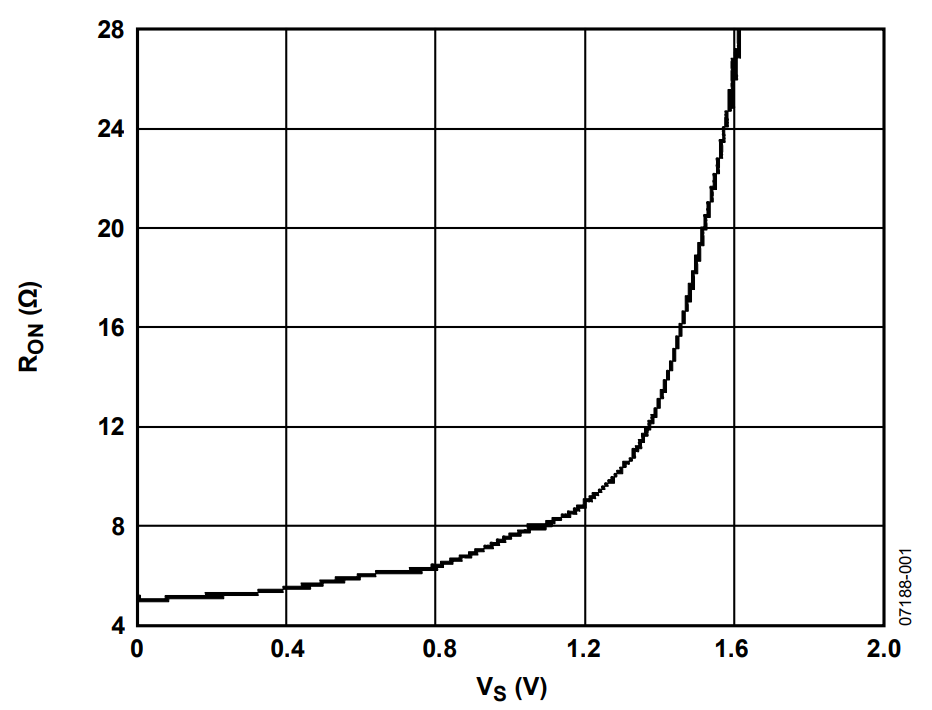
What is the on resistance for these RF switches?
Signal loss is essentially determined by the attenuation introduced by switch resistance in the on condition, RON, in series with the source-plus-load resistance, measured at the lower frequencies of operation.
The ADG9xx family uses an N-channel MOSFETs structure because this gives significant bandwidth advantages over a standard switch with NMOS and PMOS FETs in parallel. Improved bandwidth is a result of the smaller switch size and greatly reduced parasitic capacitance due to removal of the Pchannel MOSFET.
The on resistance plot for the ADG9xx matches the on resistance profile expected for an N-channel MOSFET structure. Figure 1 shows a typical RON vs. input signal plot measured on these devices.

How is high off isolation achieved?
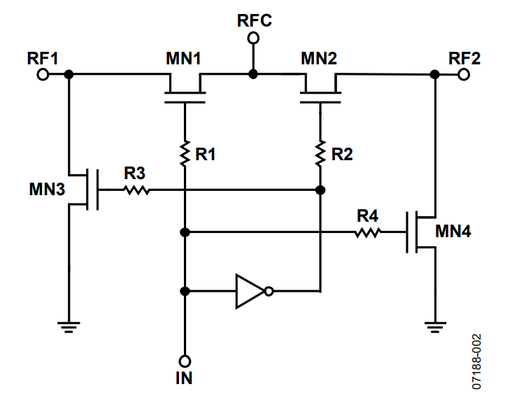
As the signal frequency increases to greater than several hundred megahertz, achieving high isolation in the off state of the switches and low insertion loss in the on state for wideband applications is a challenge for switch designers as parasitic capacitances tend to dominate.
As a departure from the familiar switch topology, inserting a shunt path to ground for the off throw (and its associated stray signal) allows the design of switches with increased off isolation at high frequencies. Figure 2 shows that the FETs have an interlocking-finger layout that reduces the parasitic capacitance between the input (RFx) and the output (RFC), thereby increasing isolation at high frequencies and enhancing crosstalk rejection. For example, when MN1 is on to form the conducting path for RF1, MN2 is off and MN4 is on, shunting the parasitics at RF2 to ground.

Why does off isolation performance decrease at lower frequencies (<1 MHz)?
Two mechanisms become significant at lower frequencies: parasitic diodes can be forward-biased and partial turn-on of the shunt NMOS device can occur when it is supposed to be off.
This has an impact on the off isolation at frequencies close to dc. These mechanisms are described in detail in the second question in the Power Handling section because they also have an effect on the power handling capability at low frequencies.
Power Handling
What is dBm?
dBm refers to decibels of power relative to 1 mW on a 50 Ω load. A 0 dBm power level is then 224 mV rms = 316 mV peak = 633 mV p-p for a sine wave signal. For other levels, the dBm measurement is:
dBm = 10 × log(P/1 mW) = 10 × log[(V rms2 )/(R × 1 mW)]
Where:
log is the base-10 logarithm.
R is 50 Ω.
Then what is a 7 dBm (5 mW) input signal? For a 50 Ω load, a 7 dBm signal corresponds to a 0.5 V rms signal, or 1.4 V p-p for sine waves. Similarly, 16 dBm corresponds to 1.4 V rms or 4 V p-p.
[V p-p = V rms × 2 × √2]
How can the part handle 7 dBm input power with no dc bias and 16 dBm input power with 0.5 V dc bias (as shown in the data sheet)?
For an input signal greater than 7 dBm, applying a 0.5 V dc bias raises the minimum level of the sine wave and prevents the negative portion of the signal from being clipped or attenuated. The small dc bias counteracts two effects that lead to the power handling capability being reduced at lower frequencies (<100 MHz).
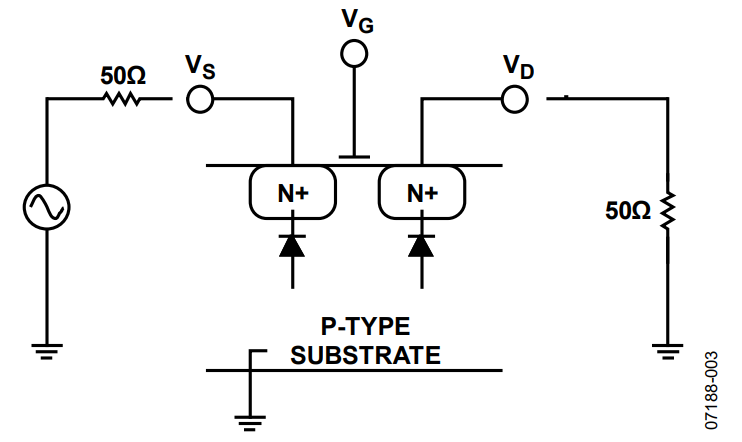
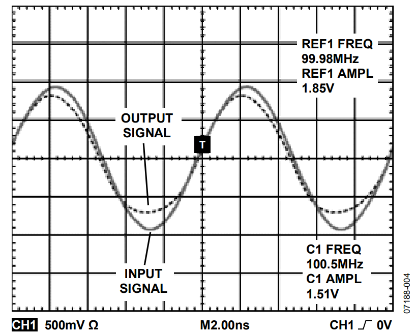
The inherent NMOS structure, as shown in Figure 3, consists of two regions of N-type material in a P-type substrate. Parasitic diodes are thus formed between the N and P regions. When an ac signal, biased at 0 V dc, is applied to the source of the transistor and VGS is large enough to turn the transistor on (VGS > VT), the parasitic diodes can be forward-biased for some portion of the negative half-cycle of the input waveform. This happens if the input sine wave goes below approximately −0.6 V, and the diode begins to turn on, thereby causing the input signal to be clipped (compressed), as shown in Figure 4. The plot shows a 100 MHz, 10 dBm input signal and the corresponding 100 MHz output signal. Note that the output signal has been truncated.


At low frequencies, the input signal is below the –0.6 V level for longer periods of time, and this has a greater impact on the 1 dB compression point (P1dB). This explains the first mechanism that leads to power handling being reduced at lower frequencies.
Parts can also handle less power at lower frequencies because of partial turn-on of the shunt NMOS device when it is supposed to be off. This is similar to the mechanism previously described where there was partial turn-on of the parasitic diode. In this case, the NMOS transistor is in the off state with VGS < VT. With an ac signal on the source of the shunt device, there is a time in the negative half-cycle of the waveform where VGS > VT, thereby partially turning on the shunt device. This compresses the input waveform by shunting some of its energy to ground.
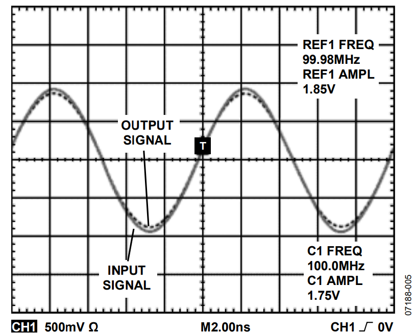
Both of the previous mechanisms can be overcome by applying a small dc bias (about 0.5 V) to the RF input signal when the switch is being used with an input signal of greater than 7 dBm (or 5 mW, 1.4 V p-p in 50 Ω). This raises the minimum level of the sine wave input signal and thus ensures that the parasitic diodes are continually reverse-biased and that the shunt transistor, never seeing VGS > VT, remains in the off state for the whole period of the input signal. Figure 5 shows a plot of input and output signals at 100 MHz and 10 dBm input power (about 2 V p-p in 50 Ω) with a 0.5 V dc bias. It is clearly visible that clipping or compression no longer occurs at 100 MHz.

How can a dc bias be applied to RF inputs?
To minimize any current drain through the termination resistance on the input side, it is best to add the bias on the output (RFC) side. This is the best practice, especially for low power portable applications, but it may be necessary to apply dc-blocking capacitors on the RF outputs if downstream circuitry cannot handle this dc bias.
Can a higher dc bias than 0.5 V be used?
Figure 1 shows that the on resistance increases exponentially as the input signal increases. It also shows that a dc signal higher than 0.5 V contributes to loss across the switch and the user will want to keep the on resistance to a minimum. As with standard CMOS switches the signal applied to the switch inputs should never exceed the VDD supply.
Author
