AN-2626: ADIN3310/ADIN6310 Schematic and System Level Design Considerations
Background
This application note serves as a guide to assist engineers during the development and review phases of schematic designs incorporating the ADIN3310/ADIN6310 Ethernet switches. It outlines key considerations and best practices to ensure robust and reliable system implementation and reduce risk of design issues.
The document is structured around four core areas: power, host interface configuration, port interfacing, and Ethernet PHY considerations. Use this document in conjunction with the ADIN3310/ ADIN6310 data sheet and hardware user guides.
Schematic Checklist
Table 1 offers a concise summary of the key considerations when developing a schematic with the ADIN3310/ADIN6310 switches. It serves as a quick reference for all the essential design elements. More detailed information is contained in the following pages.
| Sub Section | Note |
| Power Domains and Grounding | Evaluate whether separate VDDIO rails are required by the application. To reduce power consumption, use a lower voltage level, such as 1.8V or 2.5V for the VDDIO rails (VDDIO_A, VDDIO_B) instead of 3.3V. When using the ADIN6310 with all six ports at 1Gbps, VDDIO_B must be set to 1.8V or 2.5V. Operation at 3.3V is not supported due to increased power consumption over process variations, voltage tolerances, and temperature ranges. |
| Power Supply Decoupling | Each power rail requires a minimum arrangement of decoupling capacitors located as close as possible to the package balls. |
| Host Port Selection | The default host strapping configuration with no external components selects standard serial peripheral interface (SPI). Review the intended host interface mode and consider inclusion of strapping component footprints (DNI (do not install)) to allow flexibility for changes during initial prototype bring-up. |
| The TimerX and SPIx pins are referenced to the VDDIO_A power domain. Therefore, external pull-up resistors for strapping purposes must be pulled to VDDIO_A. | |
| Clocking | The switch requires a 25MHz clock, it can be a crystal or a single-ended clock. If a crystal is used, ensure the feedback resistor and drain resistors are included. |
| MAC to MAC Interface | Connect the MAC TX pins to the switch RX pins, and the MAC RX pins to the switch TX pins. |
| MAC to PHY Interface | Connect the PHY TX pins to the switch TX pins and the PHY RX pins to the switch RX pins. |
| RMII Interface | The switch port can provide the 50MHz clock required by the reduced media independent interface (RMII) to the PHY/MAC. Alternatively, an external 50MHz clock can be provided to both sides. The same clock must be used for the switch port and PHY/MAC. |
| RGMII Interface | Review the configuration of reduced gigabit media independent interface (RGMII) TXC/RXC clock delays (host interface and configured ports). Delays must be once in the path for the TXC and RXC clocks. The switch provides options to add delays in both paths as required. Evaluate inclusion of termination resistors in the RGMII paths. |
| PHY Addressing | If using ADIN1100/ADIN1101 PHYs, it is recommended to use external PHY addressing resistors. For ADIN1300 PHYs, the switch internal PHY addressing straps can provide unique PHY addresses for each port. |
| SERDES/SGMII Interface | When using serial gigabit media independent interface (SGMII), 1000BASE-KX or 100BASE-FX modes with a direct connection, external 0.1μF capacitors are required between ports. Small form-factor pluggable (SFP) modules typically include AC coupling capacitors. |
| Link Input | Dedicated Px_Link inputs must be pulled or driven low to enable each port. Ensure the polarity provided matches.
|
| Hardware Reset | Reset_N pin is active low. This pin must be driven high for normal switch operation. |
| PHY Management Interface [MDIO/MDC] | The MDIO pin requires an external 1.5kΩ resistor pulled to VDDIO_B. Only one pull-up is required, irrespective of how many PHYs the signal is routed to. Port 0 MDIO/MDC is referenced to VDDIO_A, level shifting may be required if there is a PHY connected to Port 0 and different VDDIO_A/VDDIO_B voltage rails |
| JTAG Interface | For normal operation, pull/drive TEST_EN pin low. It can be connected directly to ground if Joint Test Action Group (JTAG) interface is not required. When using JTAG, TEST_EN pin must be driven high. |
Power Domains and Grounding
This section highlights key areas to review in power supplies, decoupling and grounding. The switch has a number of power supply domains. The allowable voltage ranges for each supply rail are detailed in Table 2. It is possible to operate the switch from a minimum of two power supply rails when VDDIO_A = VDDIO_B = VDD3P3. However, use of higher VDDIO supply voltage has a direct impact on the device power consumption. It is recommended to use VDDIO at a lower supply voltage to minimize system power consumption.
| Supply | Nominal Supply | Tolerance |
| VDDIO_A | 1.8V, 2.5V, 3.3V | ±5%, ±10%, ±5%, |
| VDDIO_B | 1.8V, 2.5V, 3.3V | ±5%, ±10%, ±5%, |
| VDDCORE | 1.1V | ±5% |
| VDD3P3 | 3.3V | ±5% |
| VDD_SGMII | 3.3V | ±5% |
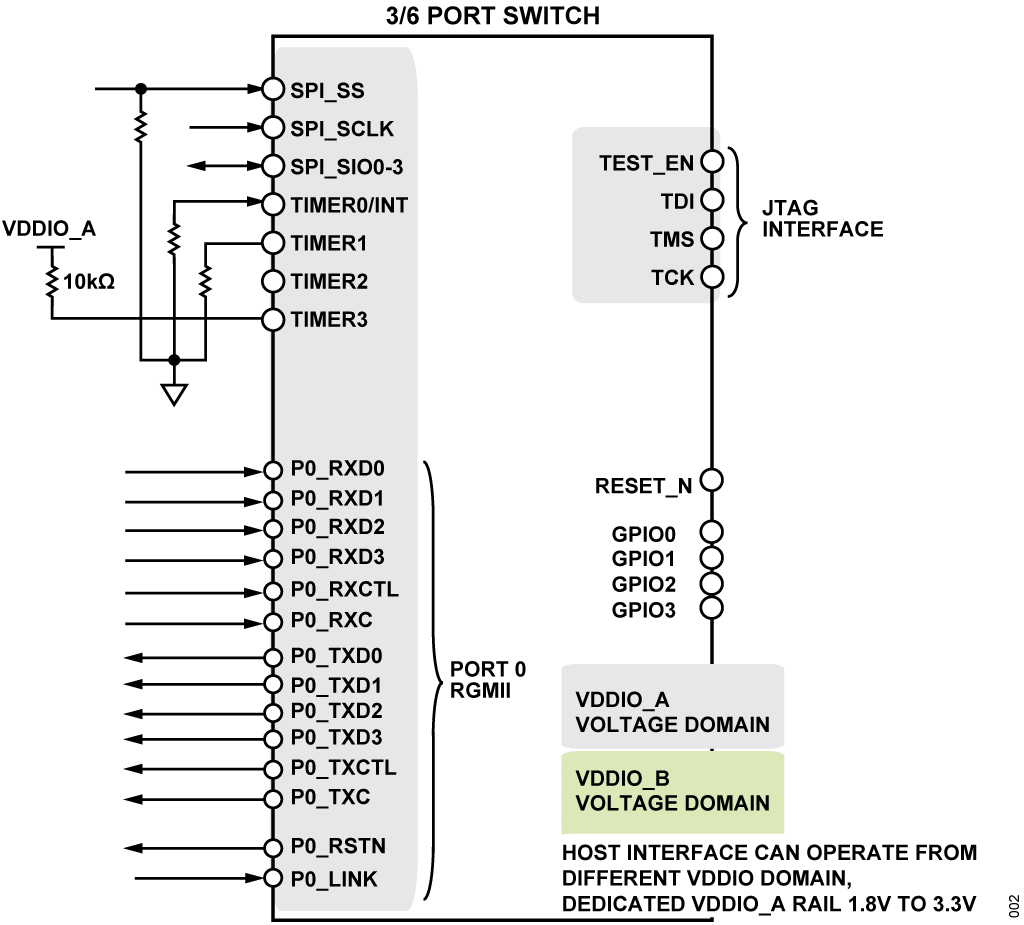
To support a host interface operating on a different I/O voltage supply, the switch allows the user to separate VDDIO into two supply domains, VDDIO_A and VDDIO_B. The VDDIO_A supply domain is used for all functions that can be connected to the host interface such as SPI, timers, GPIO, JTAG, and Port 0 MAC interface.

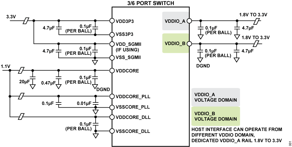
The VDDIO_B supply domain is used for all the other ports MAC interface. These ports could have Ethernet PHY devices connected to the MAC interface (such as the ADIN1100, ADIN1200, ADIN1300, or other PHYs) and the PHY VDDIO supply rail would run from the same voltage rail as the switch VDDIO_B.
If the host interface is operating from the same I/O voltage as the other ports, then connect VDDIO_A to VDDIO_B rail.

Worst-case power consumption conditions occur when all six ports operate at 1Gbps speed. For the ADIN6310, VDDIO_B is not supported at 3.3V if all six ports are being used at 1Gbps speed. In this case, VDDIO_B must operate from a 1.8V or 2.5V rail to keep the die temperature within the operating temperature range over process, temperature, and voltage tolerance.
Power Supply Decoupling
It is recommended to decouple each of the supply rails with the capacitors detailed in Table 3. When placing the decoupling capacitors, prioritize the locations detailed with capacitors connected across these nets to their relevant grounds. Place the smaller decoupling capacitor (0.1μF) as close to the relevant balls as possible and ensure the capacitor ground is routed directly into the plane.
| Supply Name | Capacitor Value | ADIN3310 | ADIN6310 |
| VDD3P3 to VSS3P3 | One 4.7μF per group, 0.1μF per ball | G4 to G3, F3 to E3, E2 to D2 | G5 to G3, J5 to J3, K5 to K3 |
| VDD_SGMII to VSS_SGMII | One 4.7μF per group, 0.1μF per ball | ||
| VDDIO_A to DGND | One 4.7μF per group, 0.1μF per ball | ||
| VDDIO_B to DGND | One 4.7μF per group, 0.1μF per ball | ||
| VDDCORE to DGND | One 20μF and 0.47μF per group, 0.1μF per ball | ||
| VDDCORE_PLL to VSSCORE_PLL | 0.1μF and 0.01μF | D4 to D3 | G5 to G3 |
| VDDCORE_DLL to VSSCORE_DLL | 0.1μF per ball | L9 to L8 | N10 to M10, D10 to E10 |
Power Supply Sequencing
There are no power sequence requirements for applying power to the switch; however, the preferred power sequence is to apply the VDDCORE supply last and remove it first.
Host Interface
The ADIN3310/ADIN6310 are managed switches and require a host to be connected over SPI or Ethernet interface to configure the switch functionality. When the switch powers up, the only interface that gets enabled is the host interface, based on the hardware strapping pins.
Host Port Selection
For Ethernet host interface, any port can be configured to serve as the host port. Port 0 is recommended as host port if the user is connecting the host to a MAC interface that runs on a different VDDIO voltage rail to the I/O voltage for the other ports. This makes use of the VDDIO_A/VDDIO_B voltage partitioning. If an Ethernet port is designated as the host interface, it can support both control and data plane traffic, therefore, can be used for data traffic to/from the host.
Strapping Pins/Host Interface Selection
There are eight pins used for host configuration strapping, the four TIMER pins (TIMER0 to TIMER3) and four SPI pins (SPI_SIO0 to SPI_SIO2, SPI_SS). On power up, the switch samples the voltage levels on these hardware strapping pins. The voltage level informs the switch core (that is, packet assist engine) how the host is connected and assigns the host communication protocol as SPI or Ethernet. The only port enabled at this point is the host interface port. All other ports remain disabled until the host calls the necessary application programming interfaces (APIs) to start switch and port configuration.
The hardware strapping pins include internal pull-up or pull-down resistors as shown in Figure 3. SPI_SIO3 and SPI_SCLK are shown in the drawing but not used for strapping purposes. With no external strapping components, the switch relies on the internal strapping which results in the default configuration of standard (single) SPI. External strapping resistors are required as shown in Table 4 to override the internal strapping and use alternative host interfaces, for example, MAC or SPI (dual or quad). TIMER0 and TIMER1 pins have internal pull-up resistors, while TIMER2 and TIMER3 have internal pull-down resistors.

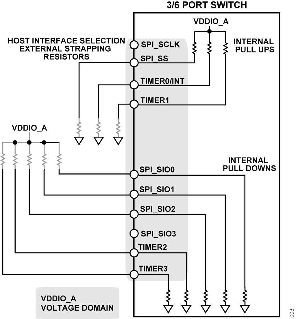
| Mnemonic | Default Configuration | External Series Resistor Required Value |
| TIMER0 | Pull-up | Pull-down <2.5kΩ to latch a value 0 |
| TIMER1 | Pull-up | Pull-down <2.5kΩ to latch a value 0 |
| TIMER2 | Pull-down | Pull-up <3.3kΩ to latch a value 1 |
| TIMER3 | Pull-down | Pull-up <3.3kΩ to latch a value 0 |
| SPI_SS | Pull-up | Pull-down <400Ω to latch a value 0 |
| SPI_SIO0 | Pull-down | Pull-up <10kΩ to latch a value 1 |
| SPI_SIO1 | Pull-down | Pull-up <10kΩ to latch a value 1 |
| SPI_SIO2 | Pull-down | Pull-up <10kΩ to latch a value 1 |
It is recommended to add resistor footprint options to allow different options for host strapping. This allows the user to make changes in event host strapping needs to be changed. For example, during initial prototype bring-up, if there are issues communicating with the switch or loading the switch firmware from the intended host, having an option to configure a different port as the host interface would allow users to load firmware using the Analog Devices, Inc., graphical user interface (GUI) through an Ethernet port to help progress debug. They could then revert to intended host as they progress proving the hardware.
The additional footprints should be left DNI (do not insert) unless required and removed in subsequent board revisions. Figure 3 shows the external resistors grayed out as they may not all be required, but it is recommended to evaluate having options to add.
The TIMER and SPI_SIOx pins are referenced to the VDDIO_A power domain, therefore external strapping resistors must be pulled to VDDIO_A.
Note the following order of steps that must be completed before the host interface can be changed:
- Power down switch.
- Update the appropriate strapping resistors by driving the voltage on their pins.
- Power up switch as the strapping pins are sampled when the device is brought out of reset.
Connected components or circuitry attached to these pins can influence the effective strapping state. Ensure that any external connections do not unintentionally alter the intended configuration. If using LEDs on the TIMER pins, review the LED circuitry to ensure it does not interfere with the intended host strapping. For example, if the intended TIMER2 voltage level is to be pulled down to 0V (as is by default), the LED circuit on the TIMER2 pin should not cause the pin to be pulled up, that is, introduce a conflict with the intended host interface.
The configuration of the SPI_SIOx pins decides which Ethernet port is host. By default, each SPI_SIOx pin is internally pulled down to set the host port as Port 0.
Table 5 provides an overview of the hardware strapping options to achieve various SPI host interface modes. As outlined, the default mode, where no external strapping resistors are applied, is standard SPI. The addition of a pull-up on TIMER3 would change the host strapping to dual SPI. The addition of a pull-up on TIMER2 would result in quad SPI with low drive strength. Pull-ups on both TIMER2 and TIMER3 provide quad SPI with high drive strength.
| Function | SPI_SIO2 | SPI_SIO1 | SPI_SIO0 | SPI_SS | TIMER3 | TIMER2 | TIMER1 | TIMER0 |
| Default Internal | Pd1 | Pd1 | Pd1 | Pu2 | Pd1 | Pd1 | Pu2 | Pu2 |
| Standard (Default) | ds3 | x4 | x4 | 1 | 0 | 0 | 1 | 1 |
| Dual | ds3 | x4 | x4 | 1 | 1 | 0 | 1 | 1 |
| Quad (Low Drive Strength) | x4 | x4 | x4 | 1 | 0 | 1 | 1 | 1 |
| Quad (High Drive Strength) | x4 | x4 | x4 | 1 | 1 | 1 | 1 | 1 |
1 Pd = Pull-down.
2 Pu = Pull-up.
3 ds = Drive strength. Two drive strength options are available for the host interface (high or low). When ds = 1, this corresponds to the higher drive strength. Drive strength for other ports can be configured through the software driver API.
4 x = Don't care.
Table 6 shows the hardware strapping arrangements required for RGMII operating host interfaces. Firstly, SPI_SIO0 to SPI_SIO2 pins provide the port selection, the default is Port 0 as all three SPI_SIOx pins have internal pull-downs. To assign any other port as the host, select the binary mapping that enables that port. For example, for Port 3 as host, configure SPI_SIO2/SPI_SIO1/SPI_SIO0 = b011 by adding pull-ups on SPI_SIO0 and SPI_SIO1. The choice of clock delays is flexible, and delays are only required once in each path. The switch can provide delays on both the transmitter and receiver. As some MACs may not have the capability to add the required delay, the switch can be configured to add the delay instead. The strapping selection here for delays and drive strength only apply for the host port. For all other ports, the driver API provides programmability. In RGMII mode, host strapping speeds of 100Mbps and 1Gbps are possible. It is not supported to configure the switch for a 10Mbps RGMII host interface.
| Function | SPI_SIO2 | SPI_SIO1 | SPI_SIO0 | SPI_SS | TIMER3 | TIMER2 | TIMER1 | TIMER0 |
| Default Internal | Pd | Pd | Pd | Pu | Pd | Pd | Pu | Pu |
| RGMII 100Mbps | ||||||||
| No Clock Delays | P2 | P1 | P0 | ds | 0 | 0 | 0 | 0 |
| Rx Clock Delay | P2 | P1 | P0 | ds | 0 | 0 | 0 | 1 |
| Tx Clock Delay | P2 | P1 | P0 | ds | 0 | 1 | 0 | 1 |
| Tx Clock Delay | P2 | P1 | P0 | ds | 0 | 0 | 1 | 0 |
| Rx and Tx Clock Delays | P2 | P1 | P0 | ds | 0 | 1 | 0 | 1 |
| RGMII 1Gbps | ||||||||
| No Clock Delays | P2 | P1 | P0 | ds | 1 | 0 | 0 | 0 |
| Rx Clock Delay | P2 | P1 | P0 | ds | 1 | 0 | 0 | 1 |
| Tx Clock Delay | P2 | P1 | P0 | ds | 1 | 0 | 1 | 0 |
| Rx and Tx Clock Delays | P2 | P1 | P0 | ds | 1 | 1 | 0 | 1 |
Table 7 provides an overview of the host strapping options for RMII interface, supporting 10Mbps and 100Mbps speeds. RMII interfaces require a 50MHz clock. The switch can provide this 50MHz clock out to the PHY (choose INT). The EXT option is where user provides an external 50MHz clock for both switch and PHY.
| Function | SPI_SIO2 | SPI_SIO1 | SPI_SIO0 | SPI_SS | TIMER3 | TIMER2 | TIMER1 | Condition |
| Default Internal | Pd | Pd | Pd | Pu | Pd | Pu | Pu | |
| RMII 10Mbps | ||||||||
| RMII CLK (INT) | P2 | P1 | P0 | ds | 0 | 1 | 0 | Internal clock output to PHY/host |
| RMII CLK (EXT) | P2 | P1 | P0 | ds | 1 | 1 | 0 | External clock source provided for PHY/host and switch |
| RMII 100Mbps | ||||||||
| RMII CLK (INT) | P2 | P1 | P0 | ds | 0 | 1 | 1 | Internal clock output to PHY/host |
| RMII CLK (EXT) | P2 | P1 | P0 | ds | 1 | 1 | 1 | External clock source provided for PHY/host and switch |
SGMII host strapping options are detailed in Table 8. Note that SGMII modes are only available on Port 1 to Port 4 for the ADIN6310, and Port 1 and Port 2 for the ADIN3310.
| Function | SPI_SIO2 | SPI_SIO1 | SPI_SIO0 | SPI_SS | TIMER3 | TIMER2 | TIMER1 | TIMER1 |
| Default Internal | Pd | Pd | Pd | Pu | Pd | Pd | Pu | Pu |
| 100BASE-FX | P2 | P1 | P0 | 0 | 0 | 0 | 1 | 1 |
| SGMII 1000Mbps | P2 | P1 | P0 | 0 | 0 | 1 | 1 | 1 |
| SGMII 100Mbps | P2 | P1 | P0 | 0 | 1 | 0 | 1 | 1 |
| 1000BASE-KX | P2 | P1 | P0 | 0 | 1 | 1 | 1 | 1 |
Hardware Reset
The RESET_N is an active low input to the switch and resides on the VDDIO_A power supply domain. The RESET_N input requires an external pull-down resistor to hold the switch in reset until the host is ready to communicate. The pin needs to be driven high for normal operation. After power on, when RESET_N is brought high and stays high, the external strapping pin states are latched.
During operation, to perform a hardware reset, the RESET_N pin must be driven low for a minimum 10μs. When asserted low, all output pins are driven to a high-Z state. The switch configuration is volatile and needs to be loaded by the host after a reset or power cycle.
Clocking
The switch requires a 25MHz clock that can be an external crystal oscillator applied across the XTAL_IN and XTAL_OUT pins or an external clock applied to the XTAL_IN pin, as shown in Figure 4.
If using an external clock, XTAL_OUT can be left open. The crystal circuit requires a number of external components, the values of which are: the feedback resistor (RF) = 1MΩ ± 5%, drain resistor (RD) = 2.1kΩ ± 5%, and C1 = C2 = 18pF.

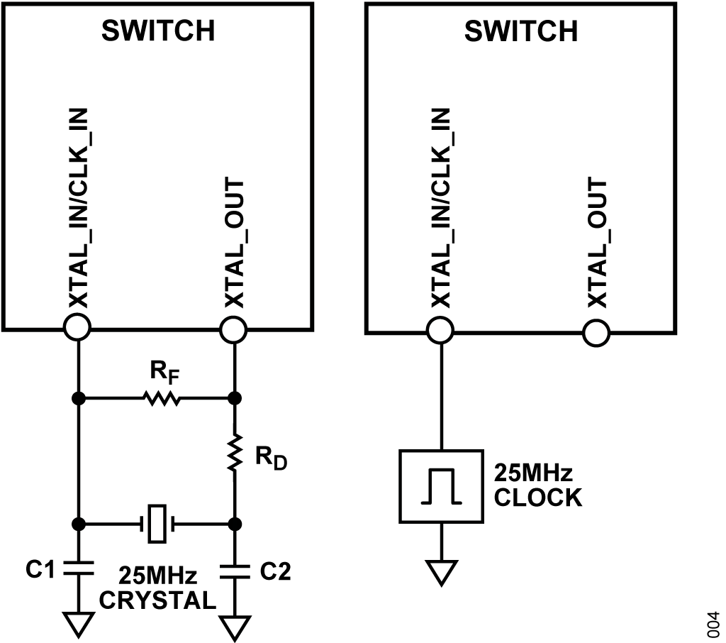
A 25MHz input clock is applied to the switch at pin XTAL_IN. This generates the 25MHz clock at the CLK_OUT pin which can be provided to the Ethernet PHY devices and requires external clock buffering. In the EVAL-ADIN6310EBZ schematic, an example of a clock buffer circuit is shown in conjunction with the switch.

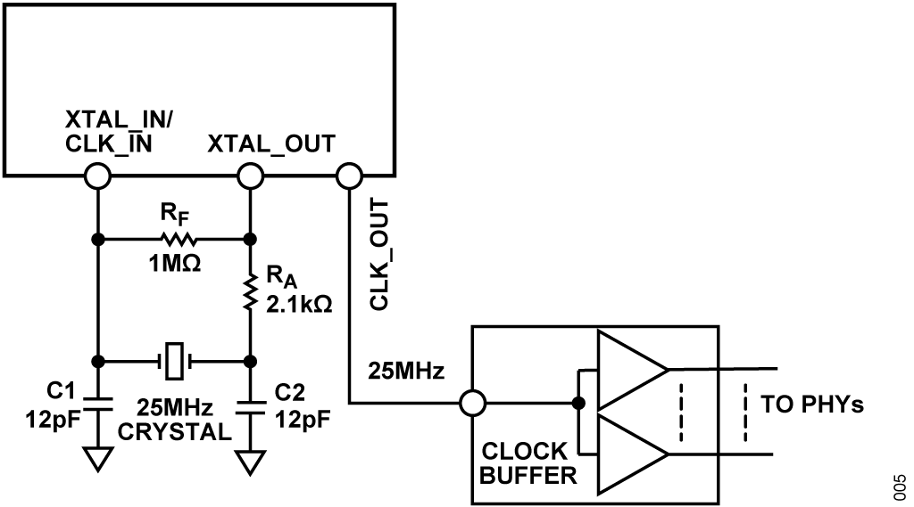
When switch ports are configured in RMII mode, the switch can generate the required 50MHz clock for use by that port and it can be provided externally to the connected MAC or PHY.
Ethernet Ports
The switches support flexible port arrangement where all ports support RMII or RGMII interfaces. The ADIN3310 Port 1 and Port 2 additionally support SGMII modes. Similarly, the ADIN6310 Port 1 to Port 4 support SGMII modes.
| ADIN3310 | ADIN6310 | Ethernet Interface Option |
| 0 | 0 | RMII, RGMII |
| 1 | 1 | RMII, RGMII, SGMII |
| 2 | 2 | RMII, RGMII, SGMII |
| N/A1 | 3 | RMII, RGMII, SGMII |
| N/A1 | 4 | RMII, RGMII, SGMII |
| N/A1 | 5 | RMII, RGMII |
1 N/A = Not applicable.
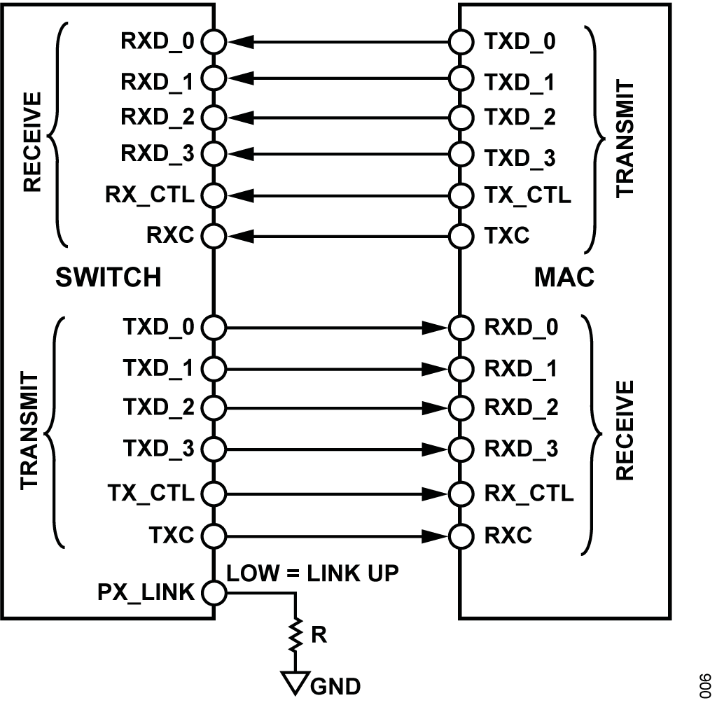
Mac to Mac Interface
The switch supports operation with a MAC to MAC interface where the switch MAC transmitter outputs are connected to the receiver inputs of the other MAC device and vice versa. When connecting MAC to MAC interfaces, care must be taken to configure both sides with matching speed and duplex. In RGMII mode, ensure a 2ns delay is introduced once in both TXC and RXC paths.

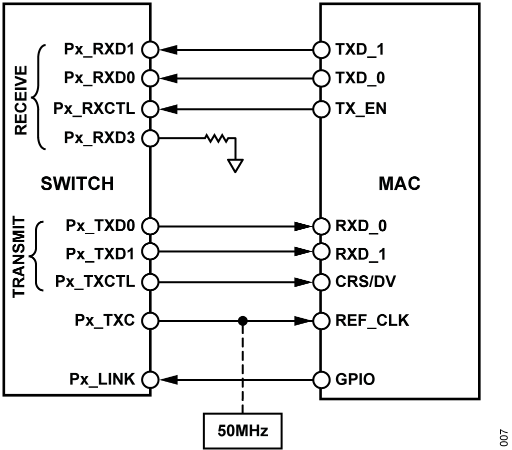
For RMII to RMII interface, the Px_RXD3 pin acts as RX_ER. If the MAC is not providing an RX_ER signal, ensure that this pin is pulled to ground. The switch can provide a 50MHz clock (on Px_TXC) to the MAC REF_CLK, or alternatively, an external 50MHz can be applied to both switch and MAC.

Connection to Ethernet Phys
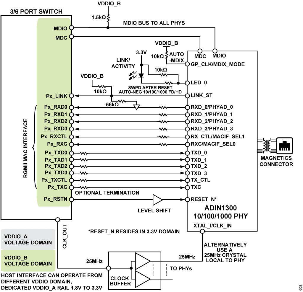
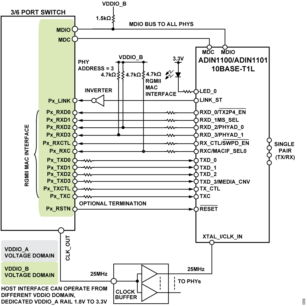
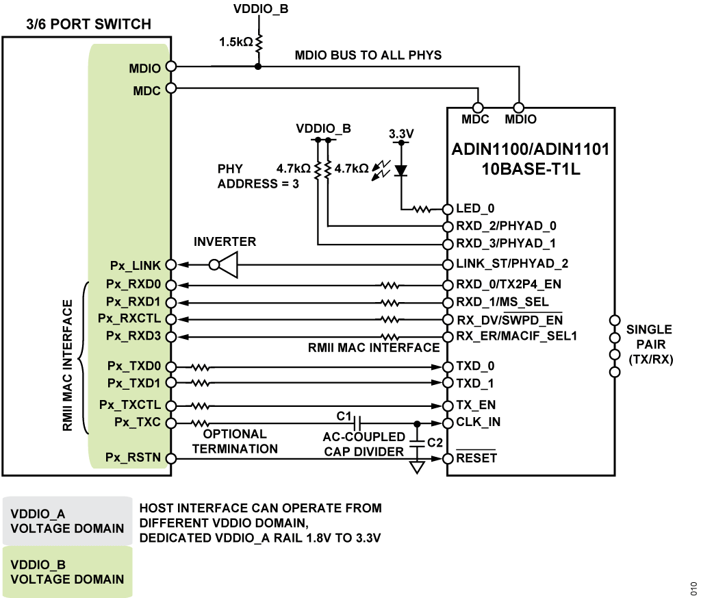
There are no Ethernet PHYs integrated into the switch, instead PHYs are placed externally and connected to each port via RMII or RGMII MAC interface. The drawing in Figure 8 shows an arrangement where an ADIN1300 10Mbps/100Mbps/1000Mbps PHY is connected to the switch RGMII port, while Figure 9 shows the ADIN1100/ADIN1101 10BASE-T1L PHY connection over RGMII and Figure 10 shows the same PHY connected over RMII.The following sections discuss the key considerations when connecting PHYs to the switch.
Mac to Phy Interface
The pin naming convention for Ethernet PHYs is different to that of the switch, with the PHY RX pins being outputs and TX pins being inputs, whereas the switches RX pins are inputs and TX pins are outputs Therefore, connect the switch RX to PHY RX and TX to TX.
It is recommended to include footprints for series termination resistors on all the output RGMII pins for both the switch and PHY. This provides options to improve signal integrity and minimize ringing as needed. Figure 8 and Figure 9 show the various connections from a switch port to the PHY.


RGMII Internal Delays
When a port is configured for RGMII interface, the switch can insert a 2ns delay in TXC and/or RXC paths to ensure proper timing alignment between clock and data signals. The delay must only be inserted once in each path. The delays can be configured for the host interface port via hardware strapping and configured for all other ports during initial configuration via software. The Ethernet PHYs do also support hardware strapping options to provide delays for TXC and RXC clocks, hence, it is important to correctly configure where the delay is added. The delays must be configured correctly on both transmitting and receiving sides to ensure successful, accurate communication.
ADIN1300 RGMII Latency Reduction
For ADIN1300 PHYs operating at 1Gbps speed, the switch automatically reduces the PHY latency if the following conditions are met: the PHY mean squared error (MSE) on all four dimensions <14 and cable length estimated by the PHY is <100m. See Table 10 for PHY latency at certain conditions.
| Tx | Rx | Condition |
| 68ns | 178ns | Low latency mode when cable length <100m and MSE value <14. |
| 68ns | 226ns | Standard latency when cable length >100m or MSE value >14 |
RMII Interface
The RMII interface requires a 50MHz clock. The switch can provide a 50MHz reference clock on its Px_TXC pin which can be used by both the switch and the PHY. Alternatively, an external 50MHz clock source can be provided to both the switch and PHY. Figure 10 shows an example of the ADIN1100/ADIN1101 PHY connected over RMII interface. Note the external resistors for PHY addressing. In this configuration the switch provides the 50MHz clock to the PHY CLK_IN. For best performance the PHY expects a clock signal of 1.0V p-p applied, therefore, a capacitor divider is recommended when using the switch to drive the 50MHz clock. The choice of C1, C2 capacitor values is discussed in detail in the PHY data sheet.

PHY Management Interface [MDIO/MDC]
The switch has a management interface that is a 2-wire bus used to manage the control and status of the external Ethernet PHYs connected to the switch MAC interfaces. The MDIO signal line must have one 1.5 kΩ pull-up resistor to the VDDIO_B voltage domain. In the event there is a PHY on Port 0, and VDDIO_A is at a different supply voltage than VDDIO_B, level shifting may be required on the MDIO bus between the voltage domains. The management interface relies on each PHY having a unique PHY address. This is discussed in the ADIN1200/ADIN1300 PHY Addressing section.
The switch can help manage the PHY configuration over the management interface (MDIO) during its port initialization routine. It can configure speed, duplex, and crossover.
During operation, the switch automatically performs read operations of Analog Devices PHYs when the link is established. It checks the speed of the established link and adjusts the switch port speed to match.
For Analog Devices ADIN product PHYs, it is recommended to hardware strap the PHYs into the software power-down mode on startup. During the switch configuration, the PHYs can be reset and brought out of software power-down mode.
Switch Port Reset Signal [PX_RSTN]
Each port has a Px_RSTN signal that can be routed to the PHY RESET_N input. By default, the switches' Px_RSTN pin is driven active low during the initial turn-on sequence. This holds the PHY in reset, until the switch is ready to configure the PHY during the switch initialize ports sequence. Only then does the switch bring the Px_RSTN line high. In the event that it is not desirable to hold the PHY in reset during this time, the reset line must not be connected to the PHY and the PHY RESET_N circuit must include an external pull-up to ensure it is possible to pull the RESET_N line high to bring the PHY out of reset.
Note that the ADIN1300 PHY RESET_N is in the AVDD3P3 voltage domain, therefore, Figure 8shows a level shifter in the path.
Switch Port Link Input
Each switch port has a dedicated Px_LINK input pin. When this pin is driven low, the port is enabled, when it is driven high the port is disabled. For ports with an Ethernet PHY connected to the port, the PHY can provide link up/link down information directly to this pin. The switch does not support in-band link or speed information. For ports connected to MAC interfaces directly, the Px_LINK input must be either pulled low with a pull-down resistor or alternatively driven low to enable the port. A logic high on the Px_LINK input disables the port.
PHY Link Signal
By default, the ADIN1101, ADIN1100, ADIN1200, and ADIN1300 PHYs drive their LINK_ST output high for link up, and low for link down. The switch expects the opposite, low for link up. For the switch port to be enabled, the Px_LINK input must be driven low. Therefore, the LINK_ST signal applied to the switch, the Px_LINK pin, must be inverted either through hardware or software. The switch does support programmatically inverting the PHY link polarity during port initialization. It interfaces directly to the PHY over the management interface and can change the polarity of the signal applied to the PHY LINK_ST pin. Alternatively, a hardware inverter can be added into the signal path between the PHY LINK_ST and Px_LINK switch input.
The EVAL-ADIN6310 schematic includes an inverter in the path between the PHY LINK_ST pin and the Port 0 P0_LINK pin. This ensures that the link information provided by the ADIN1300 PHY connected to Port 0 of the switch always matches the link polarity required by the switch. For the evaluation board specifically, this is important particularly because, by default, Port 0 is configured as the host interface port for use with the evaluation GUI, that is, the communication path between the PHY and the switch Port 0 must be established to allow the GUI communicate with the switch. For all other ports, there is no hardware inverter, and, therefore, the inversion is performed through software during the initial configuration of the ports. This has the benefit of minimizing the number of external components required in the circuit.
The EVAL-ADIN3310EBZ approach is different, in that this version of hardware includes an inverter between each PHY LINK_ST pin and the switch ports Px_LINK pin. This means the link polarity between the switch and PHY match and the switch does not need to make any changes to the link polarity in the PHY. It also means that any of the three ports could be used as the host interface as the link polarity does not need to be changed.
Similarly, for the EVAL-ADIN6310T1LEBZ (field switch) schematic, which uses a mix of the ADIN1100 and ADIN1300 PHYs, the hardware includes an inverter for each PHY LINK_ST pin and the switch ports Px_LINK pin.
ADIN1200/ADIN1300 PHY Addressing
For the ADIN1200 and ADIN1300 PHYs, PHY addressing is shared with the four RXD_x data pins. The PHYs have weak internal pull-down resistors to default to a PHY address of 0. The switch includes internal pull-up and pull-down resistors on each ports RXD pins to ensure each port provides a unique address for each PHY, which removes the requirement to have external pull-up and pull-down resistors for PHY address strapping purposes on the board. The default PHY addresses are shown in Table 11. In RGMII mode, all four RXD_x pins are connected between the switch and the PHY, and each port has a unique PHY address.
An exception to the details in Table 11 is that the PHY address of the port assigned as the host interface always gets a PHY address of 0. If the use case does have a PHY layer on the host interface and chooses a port other than Port 0 as the host interface, it is recommended to use external PHY address strapping to avoid having two PHY layers in the system with Address 0.
| Port Number | PHY Address | RXD_3 to RXD_0 |
| 0 | 0 | 0000 |
| 1 | 1 | 0001 |
| 2 | 2 | 0010 |
| 3 | 4 | 0100 |
| 4 | 8 | 1000 |
| 5 | 9 | 1001 |
When using RMII mode, the RXD_0 and RXD_1 of the PHY are connected to the corresponding Px_RXD0 and Px_RXD1 pins on the switch. The Px_RXD3 pin is now connected to RX_ER of the PHY layer. In this case, external pull-up resistors are required on RXD_2 and RXD_3 of the PHY for Port 3 to Port 5 to achieve the same port address as discussed above.
For Ethernet host connections, the expectation is that the host MAC interfaces directly to the switch MAC, with no PHY in the paths. If there is a PHY in the path, the PHY is not managed by the switch; therefore, the user must ensure that the PHY is hardware configured for the operation it requires, that is, the link signal from the PHY provides the switch with an active low for link up, and the PHY RESET_N is pulled high.
ADIN1100/ADIN1101 PHY Addressing
The PHY addressing approach for the ADIN1100/ADIN1101 PHYs uses different pins to that of ADIN1200/ADIN1300; therefore, the user must always use external PHY address strapping resistors when pairing these PHY devices with the switch.
Non-Analog Devices PHYS
It is possible to connect other vendor PHY devices to the switch ports. However, in this case, these PHYs are treated as unmanaged PHYs, and the host must take responsibility for configuring the PHY and switch port as required. The host can interface to the PHY through the switch MDIO interface and read/write registers using the SES_ReadPhyReg() and SES_WritePhyReg() APIs. When a link is established with a multispeed PHY, the host must check the PHY link speed and configure the switch port speed to match. The host can subscribe to link up/link down events for ports to help prompt managing the PHY/link.
SERDES/SGMII Interface
This interface uses two differential pairs, therefore, requires less routing and traces compared to RMII or RGMII. The switch SERDES or SGMII modes of operation support the following interface options:
- SGMII modes, support 10Mbps/100Mbps/1000Mbps speeds for copper SFPs/backplane.
- 100BASE-FX, supports 100Mbps fiber/backplane.
- 1000BASE-SX, supports 1Gbps fiber speed for short distance range of 220m to 550m.
- 1000BASE-LX, supports 1Gbps fiber speed for long distance range of up to 10km.
- 1000BASE-KX, supports 1Gbps speed for backplane applications up to 1m.
When using SGMII mode to connect to a PHY or MAC, external AC coupling capacitors are required between the devices as shown in Figure 11. Recommended values are 0.1μF. SGMII operation supports multiple speeds with auto-negotiation and forced speeds when interfaced directly to a PHY. When connected to another MAC interface, auto-negotiation must be disabled and both sides configured for the same speed. To enable the switch port for this case, the user must ensure Px_LINK is pulled low or driven low.

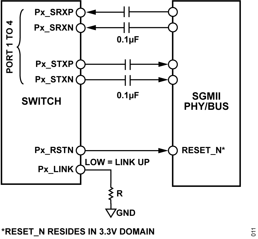
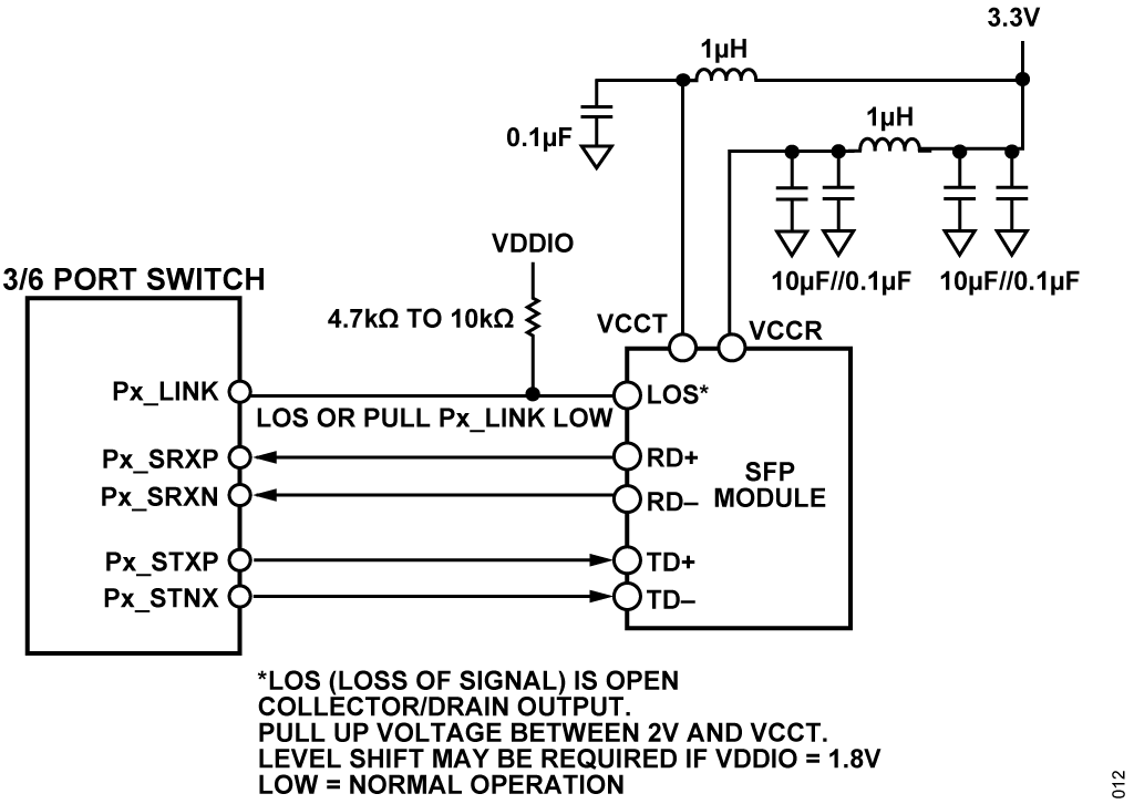
Copper/fiber SFP modules typically integrate the AC coupling capacitors. Therefore, external capacitors are not required when using these SFPs. Aside from the SFP module specific circuit, when connecting the differential pair of the SFP module to the switch, the transmit and receive paths are typically all that need to be connected, as shown in Figure 12.
To enable a port with SGMII interface, the Px_Link switch must either be pulled to ground or driven by the SFP module loss of signal (LOS). According to the SFP multiple source agreement (MSA), the LOS signal is drive high to indicate that the received optical power is too low. The signal is driven low to indicate received optical power is in normal range. The LOS output expects a pull-up voltage between 2V and the VCCT voltage level.

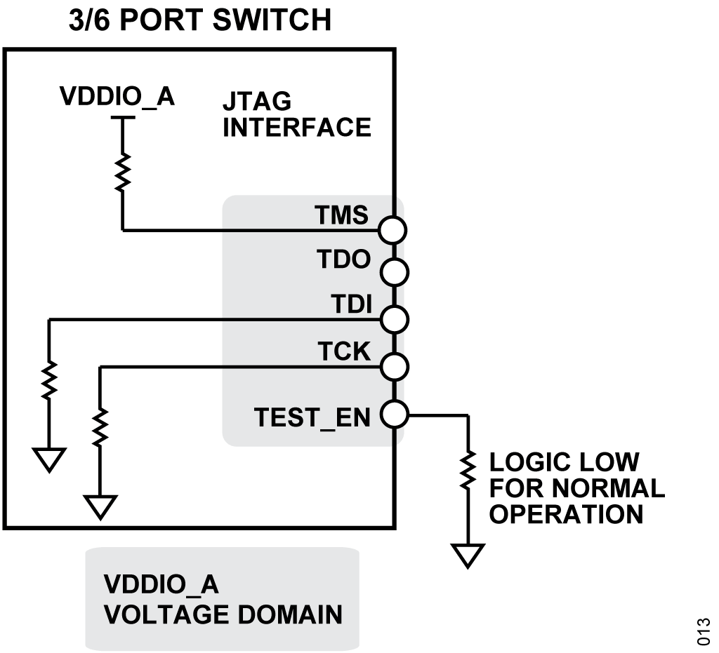
JTAG Interface
A JTAG interface is provided for the purpose of boundary scan testing, enabling verification of printed circuit board (PCB) interconnections. The JTAG pins are shared with the serial wire interface, which is used internally by Analog Devices for software development. In some of the Analog Devices schematics, the serial wire pin names are shown instead of the JTAG pin names. The serial wire interface is accessible only to Analog Devices and is locked during production testing as part of the switch security features.
The software driver package allows the host to load firmware via the configured host interface, hence, no external connectors or debuggers are required to program the switch. However, the JTAG interface remains available for customer boundary scan testing.
Normal operation of the switch requires TEST_EN to be held low (Logic 0). To enable JTAG functionality, TEST_EN must be set high (Logic 1). In the Analog Devices schematics, the TEST_EN pin is pulled to ground ensuring the switch operates in its normal mode. The TCK, TDI, and TMS pins have internal pull-up/pull-down resistors (nominal 15kΩ), therefore, if JTAG is not used, the remaining pins can remain unconnected.

Initial Firmware Load
A new switch device from the factory does not have firmware loaded. The host must be capable of loading firmware to the switch over the hardware-configured host interface, SPI or MAC. On initial boot up of a new prototype, this firmware load to the switch is the first thing the host must do. The Time Sensitive Networking (TSN) driver library includes the switch firmware as a character array in the software driver package. The size of the firmware is less than 500KB. The firmware is loaded once during the initial run, this load takes approximately 30 seconds. Once the firmware is loaded, the user can then call the APIs to configure the switch for the required functionality and port configuration. See the ADIN3310/ADIN6310 software user guide (UG-2287) for more information.
The switch configuration is volatile and must be configured by the host after each power cycle or reset.