AN-2556: IEC 61000-4-x and CISPR 11 Tested Analog Input Design with AD4116 for Industrial Automation
Introduction
The AD4116 integrates a low noise, fast settling, 24-bit Σ-Δ analog-to-digital converter (ADC) with an analog front end (AFE) for fully differential or single-ended, bipolar, ±10 V voltage inputs and five low voltage ADC inputs. The AD4116 is designed to work with programmable logic controller (PLC) and distributed control system (DCS) modules of industrial automation applications.
This application note details the functionality of the AD4116 electromagnetic compatibility (EMC) printed circuit board (PCB) that can be used with the AD4116 for a typical ±10 V voltage and ±2.5 low-voltage input. The board design demonstrates a proven EMC solution for industrial automation applications. The IEC 61000-4-x set of standards discusses the evaluation of immunity of electrical and electronic equipment at a system level.
The AD4116 EMC test board is characterized to ensure that the circuit performance is not affected by radiated radio frequency (RF) or conducted RF disturbances, and has sufficient immunity against electrostatic discharge (ESD), electrical fast transients (EFT), and surge. The board is also tested for CISPR 11, in which the radiated emissions of the board safely fall below the Class A limits.
System Design
AD4116 ADC Description
The AD4116 is a low-power, low noise, 24-bit, Σ-Δ ADC that integrates an analog front end for fully differential or single-ended bipolar, high-impedance (≥10 MΩ), bipolar ±10 V voltage inputs, and low level direct ADC inputs. The AD4116 features a maximum channel scan rate of 12.422 kSPS (80.5 µs) for fully settled data.
The embedded 2.5 V, low drift (5 ppm/°C), band gap internal reference with output reference buffer reduces the external component count. The digital filter allows flexible settings, including simultaneous 50 Hz and 60 Hz rejection at a 27.27 SPS output data rate. The user can select between the different filter settings depending on the demands of each channel in the application. An automatic channel sequencer enables the ADC to switch through each enabled channel.
The precision performance of the AD4116 is achieved by integrating the proprietary iPassives® technology from Analog Devices, Inc. The device is factory calibrated to achieve a high degree of specified accuracy. The AD4116 has the unique feature of open wire detection on the voltage inputs (patent pending) for system level diagnostics. The device can operate with a single or split power supply, making it easy to use in galvanically isolated applications.
For full details, refer to the AD4116 data sheet.
Circuit Description
The AD4116 is designed for PLC and DCS applications that are involved with harsh industrial environments. The AD4116 also satisfies the IEC 6100-4-x and CISPR 11 standards.
The circuit shown in Figure 2 demonstrates a typical multiple channel, group isolated, industrial voltage, and low input module for harsh EMI and EMC conditions using the AD4116.
In the example circuit, the ADuCM3029 ultra-low power Arm® Cortex-M3 microcontroller unit (MCU) handles local on-board control and data communication to the host computer.
The LT8301 micropower no opto isolated flyback converter and ADuM141D quad channel digital isolator enable a neat and robust solution of an isolated analog input design that operates off a single 5 V supply. The AD4116can simultaneously handle multiple voltage inputs (single-ended, bipolar differential voltage input, or low voltage differential input).
The ADP2360 high-efficiency, 60 V input voltage, discontinuous conduction mode (DCM) synchronous, step-down DC-DC switching regulator, and the ADP124 low dropout regulator (LDO) substantially simplify the on-board power supply in the example circuit to provide the necessary voltages for board functionality. The ADP2360 steps down a 6 V to 60 V input to 5 V for powering the off board serial communication function. The ADP124 regulates the ADP2360 output to 3.0 V for the ADuCM3029 microprocessor and the primary side of the ADuM141D digital isolator.
The power supplies are not intended to match the robustness of the power supply module or the backplane supply in a typical industrial automation control system. Only basic protections are implemented for the supply circuit. The AD4116 EMC test board has two options of communicating with the host computer. One is the nonisolated universal asynchronous receiver transmitter (UART) to USB port. The other option is the off board isolated UART to USB port. When undergoing the EMI and EMC testing, the AD4116 EMC test board is powered by a separate 24 V DC supply while data is sent to the host computer through the off board isolated data link.
Circuit Evaluation and Test
The AD4116 EMC test board can be run by being connected to a host computer or in standalone mode. The operational parameters are programmed in the on-board flash memory. During emission tests, the board is disconnected from the host computer while the firmware runs, and the hardware is kept operational. In the immunity tests, the board is connected to the host computer through the isolated data link. The serial port data capture program on the host computer receives ADC conversion samples from the AD4116.
The AD4116 on the EMC test board has only gone through the standard factory calibration at the component level. No further board level calibration was conducted.
The AD4116 voltage and the low-voltage analog input channel configurations are listed in Table 1. The configurations cover six typical use cases of different input types: the single-ended, high performance single-ended, differential, high performance differen tial, low level direct ADC input, and low-voltage pseudodifferential ADC input. When evaluating performance in EMC testing, VIN0, VIN2 to VIN3, VIN6, VIN8 to VIN9, VIN11 to VIN12, and VIN14 to VIN15 are supplied with the fixed voltage from the off board signal source. With the output data rate set to 1007 SPS, the AD4116 is configured to continuously sequence sample the voltage and the low-voltage ADC input channels. Further connections in EMC testing are detailed in Table 2.
| Channel | Inputs | Type | Test |
| 0 | VIN0 to VINCOM | Single-ended | Yes |
| 1 | VIN1 to VINCOM | Single-ended | No |
| 2 | VIN2 to VIN3 | Differential | Yes |
| 3 | VIN4 to VIN5 | Differential | No |
| 4 | VIN6 to VINCOM | High performance single-ended | Yes |
| 5 | VIN7 to VINCOM | High performance single-ended | No |
| 6 | VIN8 to VIN9 | High performance differential | Yes |
| 7 | VIN11 to VIN12 | Low level differential direct ADC input | Yes |
| 8 | VIN14 to VIN15 | Low-voltage pseudodifferential direct ADC input | Yes |
| AD4116 Pin | Connection in the EMC Tests |
| AVDD | 5 V |
| IOVDD | 5 V |
| AVSS | GND_ISO |
| DGND | GND_ISO |
| REF+ | Internally enabled |
| VIN0 to VINCOM | 2.5 V |
| VIN1 | GND_ISO |
| VIN2 to VIN3 | 2.5 V |
| VIN4 to VIN5 | GND_ISO |
| VIN6 to VINCOM | 2.5 V |
| VIN7 to VINCOM | GND_ISO |
| VIN8 to VIN9 | 2.5 V |
| VIN11 to VIN12 | 2.048 V |
| VIN14 to VIN15 | 2.048 V |
A 2.5 V precision signal source built with the ADR421 serves as the auxiliary equipment to provide a stable voltage reference for those ±10 V range input channels in the EMC tests. Another precision signal source with the ADR420 applies 2.048 V to the low level direct ADC input channels to suit the ±VREF range of using 2.5 V as the ADC reference.
All the selected input channels of the AD4116 were tested for each EMC test item. Before and after each possibly destructive EMC test, the board samples the 2.5 V or 2.048 V external signal source. A pair of shielded and twisted wires followed by a low-pass filter connect the output of the precision signal source to the AD4116 analog inputs. After translating the filtered signal source into voltage, the AD4116 samples from the representative channels are compared with the measurement samples of its own before the EMC transient to quantify the error and to judge the performance criterion. The deviation between the two measurements must stay within the predefined range to meet the performance criterion. The maximum allowable error is 0.1% of full scale, which aligns with the common requirements of the industrial automation applications.
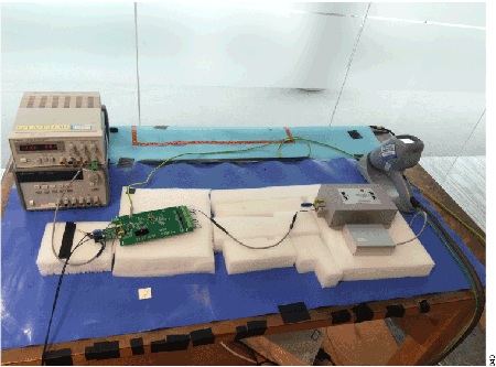
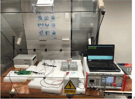
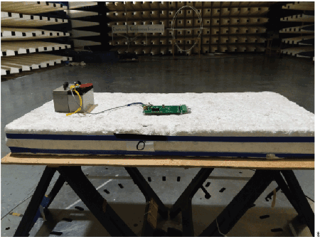
During emissions testing, the analog input channels of the board are shorted to the isolated ground. The board is disconnected from the host computer while the AD4116 keeps sampling at 1007 SPS in each channel. The only auxiliary device in this setup is a 24 V battery pack to power the EMC test board, which is assumed not to contribute EMI. The general setup for EMC testing is shown in Figure 3.
The AD4116 EMC test board is connected to the host PC via an off board optical UART to USB data link. The RealTerm software on the host computer logs AD4116 samples via this electrically isolated data link.
Software Needed
To perform EMC testing on the AD4116, the following software is required:
- Firmware Revision E8-23 on AD4116 EMC board
- RealTerm: Serial/TCP Terminal 2.0.0.70
Equipment Needed
To perform EMC testing on the AD4116, the following equipment is required:
- Optical USB transceiver board
- Industrial fiber optic cable
- PC running Windows 7, 64-bit version, image V3.0.2011.10.14
- DC power supply: Agilent 3630A, 3061A, or Yuasa NP7-12
- Precision signal source: ADR421, ADR420
- Shielded multi conductor cable (foil or braid)
- Schaffner FN353Z-30-33
Standards and Performance Criteria
The EMC and electromagnetic interference (EMI) test items, limits, and performance criteria for which this board was designed are defined according to IEC 61131-2. According to this standard, the following six applicable tests are selected:
- IEC 61000-4-2
- IEC 61000-4-3
- IEC 61000-4-4
- IEC 61000-4-5
- IEC 61000-4-6
- CISPR 11
According to these standards, the performance criteria are classified as described in Table 5.
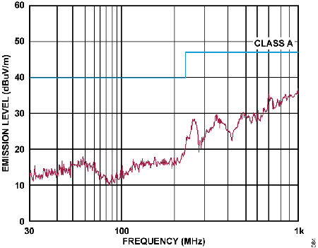
The AD4116 EMC test board was tested and has met the CISPR 11 and IEC 61000-4-x standards detailed in Table 3 and Table 4.
| Test | Basic Standard | Frequency Range | Limits | Measured Minimum Margin | Result |
| Radiated Emissions | CISPR 11 Class A | 30 MHz to 1000 MHz | See Table 12 and Table 13 | 7.7 dBµV | Pass |
| Test | Basic Standard | Test Levels | Performance Criterion | Measured Minimum Margin | Result |
| Conducted Immunity | IEC 61000-4-6 | 10 V/m | A | See Table 6 | Pass |
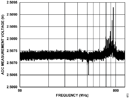
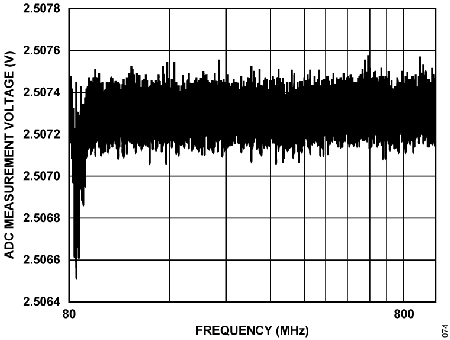
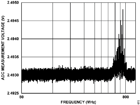
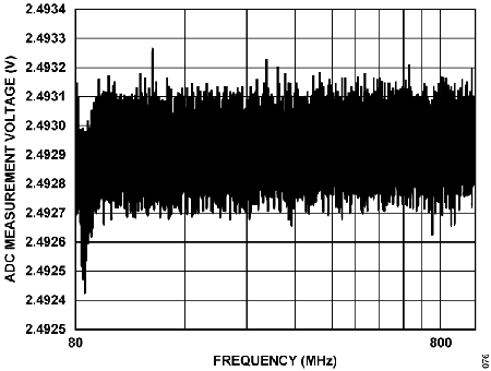
| Radiated Immunity | IEC 61000-4-3 | 10 V/m | A | See Table 11 | Pass |
| ESD | IEC 61000-4-2 | ±6 kV | B | See Table 7 | Pass |
| EFT | IEC 61000-4-4 | ±4 kV | B | See Table 8 | Pass |
| Surge | IEC 61000-4-5 | ±2 kV | B | See Table 10 | Pass |
| Performance Criterion | Description |
| A | Normal performance within an error band specified by the manufacturer. |
| B | Temporary loss of function or degradation of performance, which ceases after the disturbance is removed. The equipment under test recovers its normal performance without operator intervention |
| C | Temporary loss of function or degradation of performance, correction of performance requires operator intervention such as manual restart, power-off, or power-on |
| D | Loss of function or degradation of performance, which is not recoverable. Permanent damage to hardware or software, or loss of data. |
Printed Circuit Board
The AD4116 EMC test board is a separate design from the standard AD4116 evaluation board EVAL-AD4116ASDZ, which is designed to give optimum ADC performance but may not be optimized for EMC and EMI testing.
The AD4116 EMC test board is built on an FR4 4-layer PCB. The PCB stack up is shown in Figure 4. Both the primary side and the secondary side have 0.5 oz copper foil. The system side of the board (consisting of the LDOs, the microprocessor, the primary side of the ADuM141D, and the UART to USB transceiver) sits on the 4-layer structure. The internal layers are on 1 oz copper. These layers are designed to provide the optimum EMC and EMI performance on the portion of the board that does not directly host the AD4116.
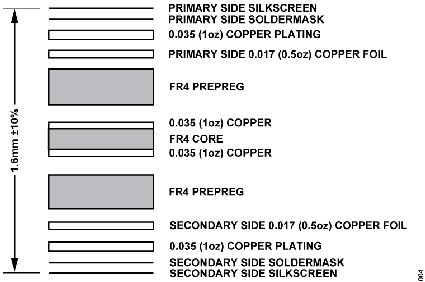
The field side of the EMC board, including the AD4116 and its entire periphery, sits on a pseudo 2-layer structure where the inner layers for the ground plane and the power plane are completely etched out. These layers are designed to demonstrate the feasibility for the AD4116 to achieve its specified functional performance, as well as EMC and EMI performance on a low cost 2-layer PCB.
Component Placement and Layout Considerations
Because the resolution of the high resolution of and low noise levels from the AD4116, take care with regard to decoupling, grounding, and layout. The analog and digital sections are separated on the EMC board and confined to certain areas of the board. The AD4116 is placed on one solid ground plane, to which both the AVSS and DGND pins are soldered when a printed circuit board with more than two layers is used. The digital interface side of the AD4116 is located close to the isolators, and the analog side faces the voltage and low-level voltage terminal blocks. The power supplies are decoupled with a 0.1 μF capacitor in parallel with a 10 nF capacitor. Both are low equivalent series resistance (ESR) ceramic capacitors in a surface-mount footprint and located as close as possible to the AD4116 power supply pins.
The damping resistors attenuate the electrical transients from tens of ohms to hundreds of ohms on the digital lines due to the comple mentary metal-oxide semiconductor (CMOS) switching on and off, helping to reduce EMI. The resistors can also reduce the ringing caused by adding ferrite beads in the serial peripheral interface (SPI).
This board used the LT8301 micropower no opto isolated flyback converter, shown in Figure 5, to generate the isolated 5 V across the isolation barrier for the AD4116. Efforts are made to keep the loop area consisting of the LT8301 SW pin (Pin 4), the T1 power transformer, and the C48 stitching capacitor connecting the primary ground (DGND) and the isolated ground (GNDISO) as small as possible to minimize EMI. Application details for the LT8301 can be found in the LT8301 data sheet.

Take care to follow the recommendations in the ADuM141D data sheet to achieve improved radiated emissions performance. A parallel combination of at least two capacitors between the VDD1 pin and GND1 pin, and between the VDD2 pin and GND2 pin, is used to suppress noise and reduce ripple. The 0.1 μF and 10 nF low ESR ceramic capacitors provide low inductance in high frequencies. Both these capacitors are placed as close as possible to the ADuM141D power pins, with PCB traces of minimum length. The VDD1 pin shares a 10 μF buck capacitor with the upstream power supply for ripple suppression and proper regulation. The VDD2 pin shares a 10 μF buck capacitor with the upstream power supply for ripple suppression and proper regulation.
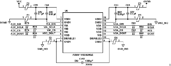
Surface-Mount Ferrite Bead BLM18HE152SN1D is placed in series with the VDD1 and GND1 pins, and the VDD2 and GND2 pins to increase the impedance to high frequency currents. The ferrite bead typically has 2 kΩ impedance from 100 MHz to 1 GHz, which can reduce the emissions at the 125 MHz primary switching frequency and the 250 MHz secondary side rectifying frequency and harmonics. In the AD4116, the IOVDD pin powers VDD2 via a short trace. GND2 (Pin 15) is connected to other GND2 (Pin 9) internally. Pin 15 is wired to the bypassing capacitors and GND_ISO via the ferrite bead as shown in Figure 6. GND2 (Pin 9) has three connections. The first connection is wired to the GND_ISO through the ferrite bead. The second connection pulls Pin 10 low, which is DISABLE2. The third connection is a high voltage surface-mount technology (SMT) capacitor is connected directly between GND2 (Pin 9) and GND1 (Pin 8) for optimal performance. For additional reduction in emissions, PCB stitching capacitance can be implemented, as detailed in AN-0971.
Other Component Considerations
The AD4116 EMC test board uses 0.1 µF, 50 V/X5R, 10%, low ESR ceramic capacitors in a C0402 footprint for the decoupling capacitors on the field side of the board. The use of ESR capacitors is a trade-off among considerations for performance, derating, cost, and space-saving. The decoupling capacitors on the system microprocessor side use 0.1 µF, 50 V/X7R, 10%, low ESR ceramic capacitors in a C0603 footprint.
Voltage Supply Protection
The scope of EMC and EMI evaluation and demonstration is focused on the AD4116 and its companion parts. The power supply circuits on the AD4116 EMC test board provide the necessary voltages for board functionality. The supply circuits are not intended to match the robustness of the power supply module or the back plane supply in an industrial automation control system. As such, only basic protections are implemented for these supply circuits. A 1 nF capacitor is placed next to each pin of the power input terminal to the protected ground, where transient energy can be discharged to the earth ground through a 3.3 nF/3 kV capacitor. The 4.7 MΩ resistor bleeds the energy to the earth that may be accumulated on the protected ground. A diode is inserted to protect the miswiring to the power supply input. The SMBJ26CA transient voltage suppression (TVS) diode clamps the transient voltage from going higher than 24 V (nominal). A common-mode inductor blocks the emissions escaping from the downstream circuits. A second SMBJ26CA TVS diode after the inductor provides further clamping for the transient.
ESD Protection
Appropriate ESD protection circuitry must exist on the EMC test board. The protection consists of a current limiting resistor, a transient voltage clamp, and a transient energy diverting capacitor.
There are three minimum mandatory components for AD4116 EMC and EMI in the voltage input channels: a 180 Ω resistor, a 4.7 nF capacitor, and a TVS device. The 180 Ω resistor on the trace between the AD4116 VINx pin and the terminal block in conjunction with the 4.7 nF/50 V C0G GRT155R71H472KE01D capacitor provides antialias filtering for the ADC. The RC filter can attenuate the RF interferences during the EMC testing. Because the AD4116 VINx pins are internally connected to ~1 MΩ resistors, the 180 Ω serial resistor provides some little additional isolation between the AD4116 and the high voltages that the TVS clamps. The TVS device is crucial to clamp the electrical transient on the board during the EMC events. An SMAJ33CA-TR is inserted between the AD4116 and the input terminal block. The TVS pins are routed to the VINx terminal pins with short and heavy traces.
There are three minimum mandatory components for the AD4116 EMC and EMI in the low-level direct ADC input channels: a TVS device, a 3 kΩ resistor, and a 270 pF capacitor. The 3 kΩ resistor on the trace between the AD4116 ADCINx pin and the terminal block helps to limit the transient current to and from the part. The TVS device is crucial to clamp the electrical transient on the board during the EMC events. An SMAJ10CA-TR is inserted after the input terminal block and before the current limiting resistor. The TVS pins are routed to the ADCINx terminals with short and heavy traces. A 270 pF/50 V X7R GCM155R71H271KA37D capacitor located after the current limiting resistor diverts the small amount of high-frequency transient to the isolated ground.
EMC and EMI Measurement Results of the AD4116 EMC Test Board
Conducted Immunity
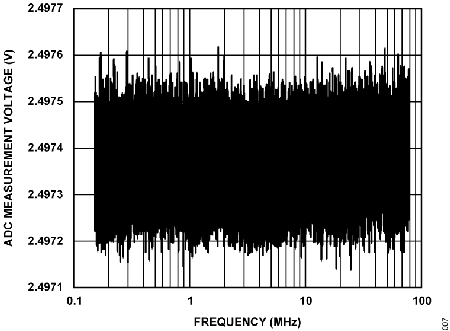
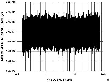
As per IEC 61000-4-6, the equipment under test (EUT) is placed on an insulating support of 0.1 meter height above a ground reference plane. All cables exiting the EUT are supported at a height of at least 30 mm above the ground reference plane. The interference is injected with a coupling/decoupling network (CDN) KEMZ 801A. The cable is decoupled by an attenuation clamp, KEMZ 801A. The frequency range is swept from 150 kHz to 80 MHz (10 V/m) with the disturbance signal of 80% amplitude modulated with a 1 kHz sine wave. The step size is 1% of the start and thereafter 1% of the preceding frequency value where the frequency is swept incrementally. The dwell time of the amplitude modulated carrier at each frequency is 1 sec.
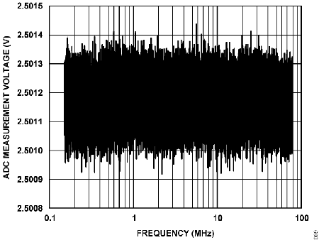
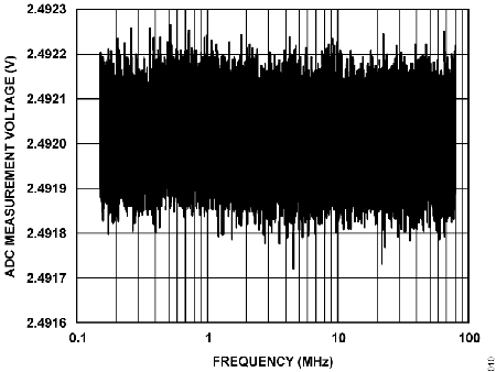


| Input Channel | Average (V) | During Zap | Deviation | Pass or Fail | |
| Min (V) | Max (V) | ||||
| VIN0 | 2.497386 | 2.497134 | 2.497619 | −24 ppm, 23 ppm × full scale (FS) | Pass, Criterion A |
| VIN2 to VIN3 | 2.491699 | 2.491963 | 2.491418 | −28 ppm, 26 ppm × FS | Pass, Criterion A |
| VIN6 | 2.501158 | 2.500901 | 2.501434 | −26 ppm, 28 ppm × FS | Pass, Criterion A |
| VIN8 to VIN9 | 2.492011 | 2.491722 | 2.492264 | −29 ppm, 25 ppm × FS | Pass, Criterion A |
| ADCIN10 to ADCIN12 | 2.048039 | 2.047929 | 2.048115 | −21 ppm, 15 ppm × FS | Pass, Criterion A |
| ADCIN14 to ADCIN15 | 2.047228 | 2.047156 | 2.047260 | −13 ppm, 6 ppm × FS | Pass, Criterion A |
Immunity to ESD
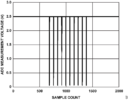
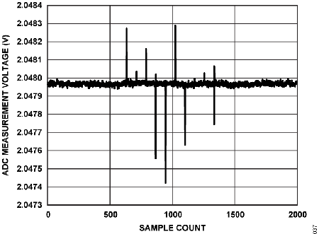
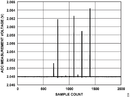
As per IEC 61000-4-2, the test setup consists of a nonconductive table, 0.8 meters high, standing on the ground reference plane. A horizontal coupling plane (HCP) of 1.6 meters × 0.8 meters is placed on the table. The EUT and its cable are isolated from the coupling plane by an insulating mat 0.5 mm in thickness. The contact discharges are applied to the VINx and ADCINx screws of the AD4116 input terminal block. The EUT is exposed to at least 20 discharges at each rating, 10 each at negative and positive polarity. The discharges are repeated at 1 per second.


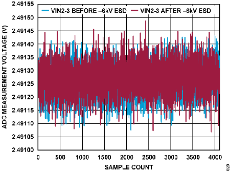
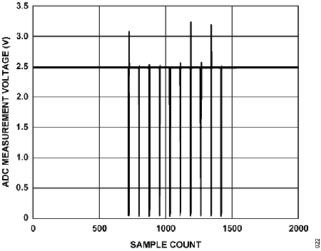
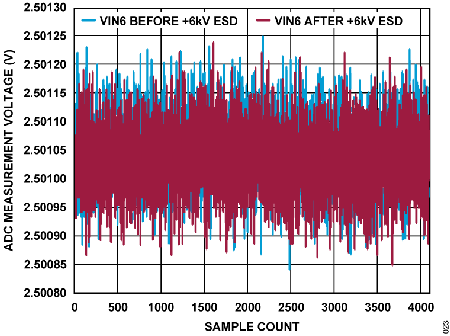
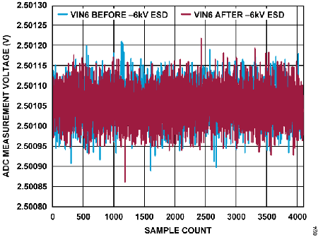
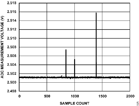
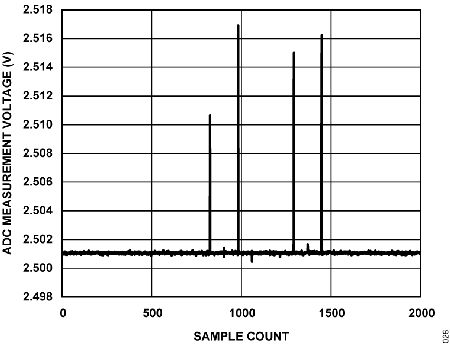
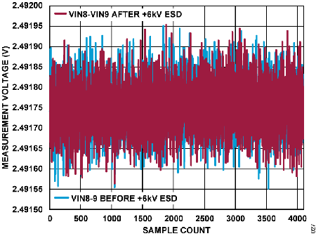
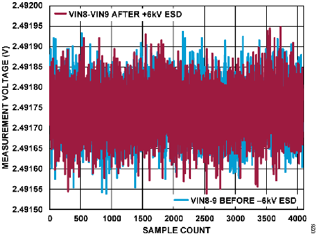
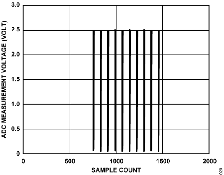
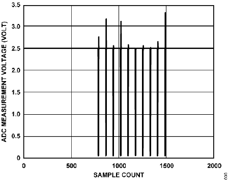
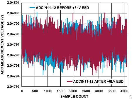
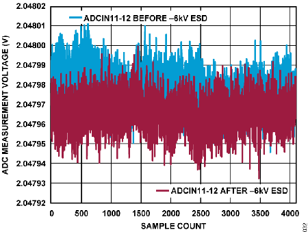

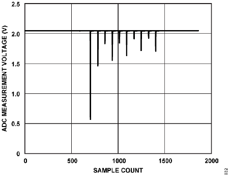
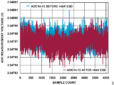
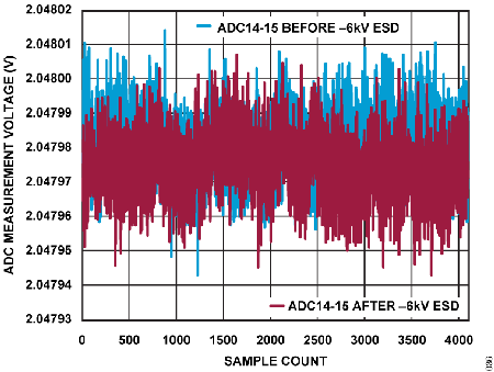
| Input Mode | Zap Point | Test Level (kV) | Before Zap (V) | After Zap (V) | Deviation (ppm) | Pass or Fail |
| Single-Ended Voltage | VIN0 | 6 | 2.497231 | 2.497237 | 2 | Pass, Criterion B |
| −6 | 2.497255 | 2.497253 | −1 | Pass, Criterion B | ||
| High Performance Single Ended Voltage | VIN6 | 6 | 2.501055 | 2.501037 | −7 | Pass, Criterion B |
| −6 | 2.501060 | 2.501051 | −3 | Pass, Criterion B | ||
| Differential Voltage | VIN2 to VIN3 | 6 | 2.491270 | 2.491272 | 1 | Pass, Criterion B |
| −6 | 2.491261 | 2.491273 | 5 | Pass, Criterion B | ||
| High Performance Differential Voltage | VIN8 to VIN9 | 6 | 2.491753 | 2.491750 | −1 | Pass, Criterion B |
| −6 | 2.491748 | 2.491741 | −3 | Pass, Criterion B | ||
| Low Level Differential Direct ADC Input | VIN11 to VIN12 | 6 | 2.047971 | 2.047971 | 1 | Pass, Criterion B |
| −6 | 2.047979 | 2.047966 | −6 | Pass, Criterion B | ||
| Low Level Pseudodifferential Direct ADC Input | VIN14 to VIN15 | 6 | 2.047974 | 2.047970 | −2 | Pass, Criterion A |
| −6 | 2.047982 | 2.047975 | −3 | Pass, Criterion B |
| Input Mode | Zap Point | Test Level (kV) | Before Zap (V) | During Zap (V) | Deviation | |
| Min | Max | |||||
| Single-Ended Voltage | VIN0 | 6 | 2.497231 | 2.496880 | 2.504259 | −0.01%, 0.28% |
| −6 | 2.497255 | 2.497032 | 2.539483 | −0.01%, 1.69% | ||
| High Performance Single Ended Voltage | VIN6 | 6 | 2.501055 | 2.500749 | 2.515745 | −0.01%, 0.59% |
| −6 | 2.501060 | 2.500495 | 2.516893 | −0.02%, 0.63% | ||
| Differential Voltage | VIN2 to VIN3 | 6 | 2.491270 | 0.042328 | 2.492180 | −98.30%, 0.04% |
| −6 | 2.491261 | 0.042990 | 3.230697 | −98.27%, 29.68% | ||
| High Performance Differential Voltage | VIN8 to VIN9 | 6 | 2.491753 | 0.032002 | 2.503461 | −98.72%, 0.47% |
| −6 | 2.491748 | 0.032106 | 3.308076 | −98.71%, 32.76% | ||
| Low Level Differential Direct ADC Input | VIN11 to VIN12 | 6 | 2.047971 | 0.689038 | 2.048014 | −66.36%, 21 ppm |
| −6 | 2.047979 | 0.559444 | 2.048068 | −72.68%, 44 ppm | ||
| Low Level Pseudodifferential Direct ADC Input | VIN14 to VIN15 | 6 | 2.047974 | 2.047422 | 2.048288 | −0.03%, 0.02% |
| −6 | 2.047982 | 2.047763 | 2.064334 | −0.01%, 0.80% | ||
Immunity to Electrical Fast Transients
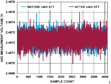
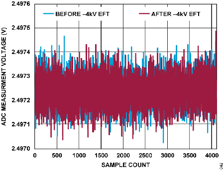
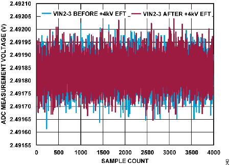
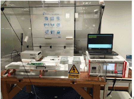
As per IEC 61000-4-4, the EUT is tested with 2000 V discharges on the analog input cable. Both positive and negative polarity discharges are applied. The length of the hot wire from the coaxial output of the EFT generator to the terminals on the EUT must not exceed 1 meter. The duration time of each test sequential is 1 minute. The transient and burst waveform is in accordance with IEC 61000-4-4, 5/50 ns.
The configuration consists of a wooden table 0.8 meters high covered with a sheet of copper at least 0.25 mm thick connected to the protective grounding system. The EUT is placed on a 0.1 meters thick isolating support. A minimum distance of 0.5 meters is provided between the EUT and the walls of the laboratory.
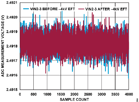
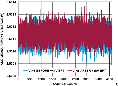
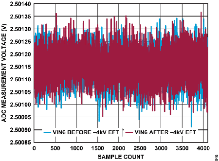
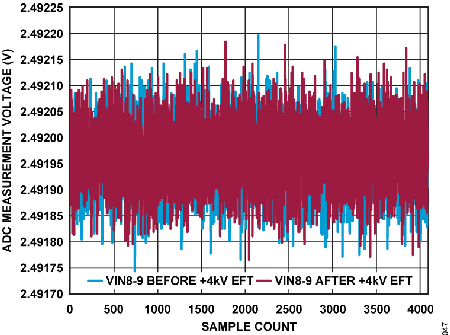


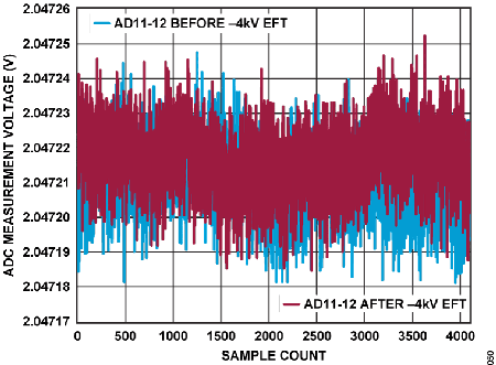
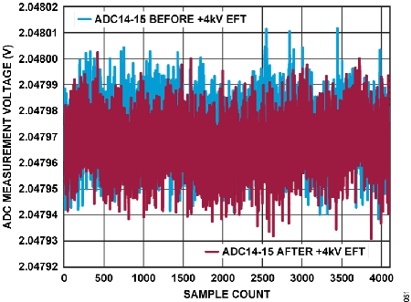
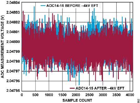
| Input Mode | Zap Point | Test Level (kV) | Before Zap (V) | After Zap (V) | Deviation (ppm) | Pass or Fail |
| Single-Ended Voltage | VIN0 | 4 | 2.497243 | 2.497235 | −3 | Pass, Criterion B |
| −4 | 2.497245 | 2.497237 | −3 | Pass, Criterion B | ||
| High Performance Single Ended Voltage | VIN6 | 4 | 2.501117 | 2.501143 | 10 | Pass, Criterion B |
| −4 | 2.501151 | 2.501156 | 2 | Pass, Criterion B | ||
| Differential Voltage | VIN2 to VIN3 | 4 | 2.491827 | 2.491833 | 3 | Pass, Criterion B |
| −4 | 2.491818 | 2.491817 | −1 | Pass, Criterion B | ||
| High Performance Differential Voltage | VIN8 to VIN9 | 4 | 2.491958 | 2.491968 | 4 | Pass, Criterion B |
| −4 | 2.491972 | 2.491972 | −1 | Pass, Criterion B | ||
| Low Level Differential Direct ADC Input | VIN11 to VIN12 | 4 | 2.047200 | 2.047195 | −3 | Pass, Criterion B |
| −4 | 2.047211 | 2.047217 | 3 | Pass, Criterion B | ||
| Low Level Pseudodifferential Direct ADC Input | VIN14 to VIN15 | 4 | 2.047973 | 2.047967 | −3 | Pass, Criterion B |
| −4 | 2.047997 | 2.047994 |
2 | Pass, Criterion B |
Immunity to Surge
As per IEC 61000-4-5, the surge is a combination wave of 1.2 µS and 50 µS open circuit voltage, 8 µS and 20 µS short-circuit current. The EUT is subject to five positive and five negative surges at each rating. The interval between each surge is 1 minute. The surge is tested to the AD4116 input cable, which is treated as shielded asymmetrically operated interconnection lines of the EUT. The surge is applied to the cable shield via the capacitive coupling. The coupling and decoupling networks cannot influence the specified functional conditions of the EUT. The interconnection line between the EUT and the coupling and decoupling networks is 2 meters in length (or shorter).
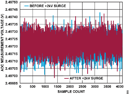
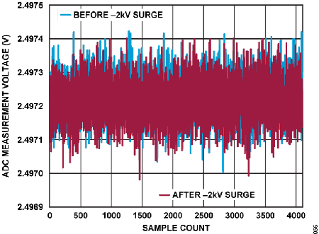

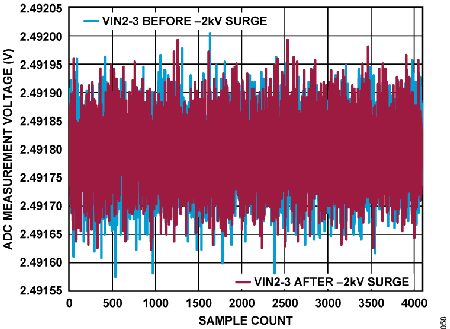
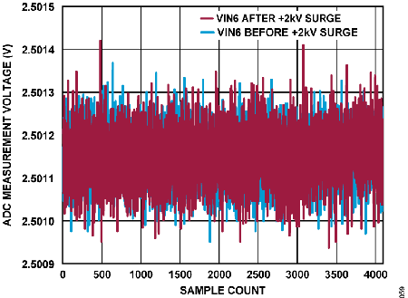


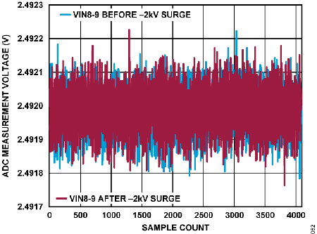

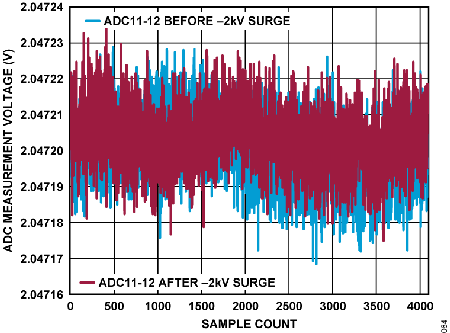
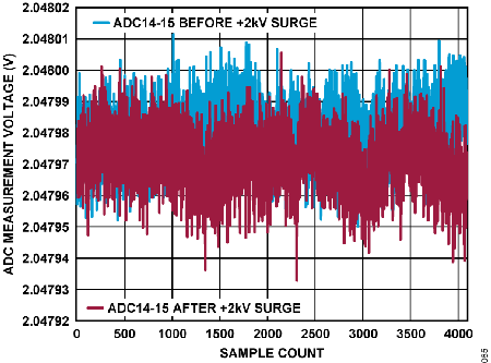
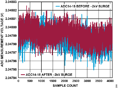

| Input Mode | Zap Point | Test Level (kV) | Before Zap (V) | After Zap (V) | Deviation (ppm) | Pass or Fail |
| Single-Ended Voltage | VIN0 | 2 | 2.497199 | 2.497218 | 7 | Pass, Criterion B |
| −2 | 2.497228 | 2.497217 | 5 | Pass, Criterion B | ||
| High Performance Single Ended Voltage | VIN6 | 2 | 2.501149 | 2.501149 | −1 | Pass, Criterion B |
| −2 | 2.501135 | 2.501134 | −1 | Pass, Criterion B | ||
| Differential Voltage | VIN2 to VIN3 | 2 | 2.491764 | 2.491770 | 3 | Pass, Criterion B |
| −2 | 2.491789 | 2.491794 | 2 | Pass, Criterion B | ||
| High Performance Differential Voltage | VIN8 to VIN9 | 2 | 2.491997 | 2.491995 | −1 | Pass, Criterion B |
| −2 | 2.491979 | 2.491988 | 4 | Pass, Criterion B | ||
| Low Level Differential Direct ADC Input | VIN11 to VIN12 | 2 | 2.047188 | 2.047186 |
−1 | Pass, Criterion B |
| −2 | 2.047200 | 2.047204 | 2 | Pass, Criterion B | ||
| Low Level Pseudodifferential Direct ADC Input | VIN14 to VIN15 | 2 | 2.047980 | 2.047971 | −5 | Pass, Criterion B |
| −2 | 2.047987 | 2.047991 |
2 | Pass, Criterion B |
Radiated Immunity
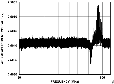
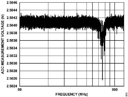
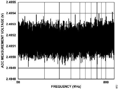
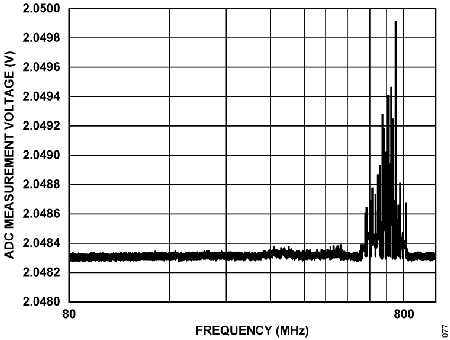
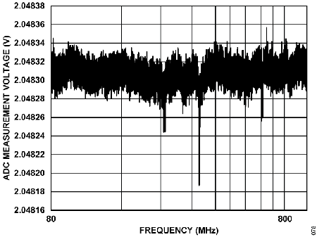
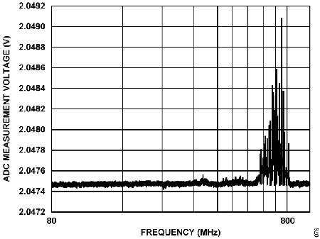
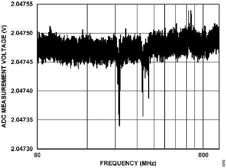
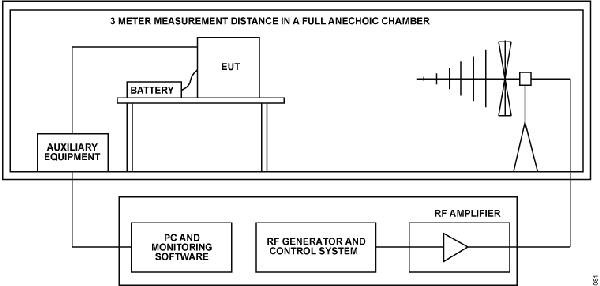
As per IEC 61000-4-3, the test is performed in a fully anechoic chamber. The EUT is placed on a nonconductive table 0.8 meters in height. The AD4116 inputs are shorted to its isolated ground. The transmit antenna is located at a distance of 3 meters from the EUT. The frequency range is swept from 80 MHz to 1000 MHz with the signal 80% amplitude modulated with a 1 kHz sine wave. The frequency range is swept incrementally, and the step size is 1% of the preceding frequency value. The dwell time at each frequency is 1 sec, and cannot be less than the time necessary for the EUT to respond. The field strength is 10 V/m. The test is performed with the EUT exposed to both a vertically and horizontally polarized field. The AD4116 samples are sent to the host PC that is outside of the chamber through an optically isolated data link.


| Input Channel | Antenna Polarization | Average (V) | During Zap | Deviation | Pass or Fail | |
| Min (V) | Max (V) | |||||
| VIN0 | Horizontal | 2.504096 | 2.503377 | 2.505389 | −0.03% to 0.05% | Pass, Criterion A |
| Vertical | 2.504096 | 2.502570 | 2.504322 | −0.06% to 0.01% | Pass, Criterion A | |
| VIN2 to VIN3 | Horizontal | 2.507297 | 2.506512 | 2.509287 | −0.03% to 0.08% | Pass, Criterion A |
| Vertical | 2.507304 | 2.506512 |
2.507576 | −0.03% to 0.01% | Pass, Criterion A | |
| VIN6 | Horizontal | 2.495164 | 2.494913 | 2.496603 | −0.01% to 0.06% | Pass, Criterion A |
| Vertical | 2.495155 | 2.494910 | 2.495411 | −0.01% to 0.01% | Pass, Criterion A | |
| VIN8 to VIN9 | Horizontal | 2.493020 | 2.492785 | 2.494824 | −0.01% to 0.07% | Pass, Criterion A |
| Vertical | 2.493011 | 2.492601 | 2.493286 | −0.02% to 0.01% | Pass, Criterion A | |
| ADCIN10 to ADCIN12 | Horizontal | 2.048316 | 2.048275 | 2.049910 |
−20 ppm, 0.08% | Pass, Criterion A |
| Vertical | 2.048304 | 2.048187 | 2.048356 | −0.01%, 25 ppm | Pass, Criterion A | |
| ADCIN14 to ADCIN15 | Horizontal | 2.047489 | 2.047421 | 2.049078 | −33 ppm, 0.08% | Pass, Criterion A |
| Vertical | 2.047477 | 2.047340 | 2.047538 |
−0.01%, 30 ppm | Pass, Criterion A | |
Radiated Emissions
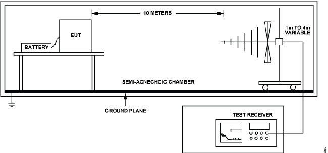
As per CISPR 11, the EUT is placed on the top of a rotating table 0.8 meters above the ground in a 10 meters semianechoic chamber. The table is rotated 360° to identify the position of the highest radiation. The EUT is set 10 meters away from the interference receiving antenna, which can be set to a horizontal or vertical polarization position. The antennas are mounted on the top of a variable height antenna tower. The heights of the antennas vary from 1 meter to 4 meters above the ground to identify the maximum value of the field strength. The EUT is configured to its worst case, the antenna is tuned to a height from 1 meter to 4 meters, and the table is turned from 0º to 360º to find the maximum reading. The test receiver system is set to quasi-peak detection mode. The EUT is powered by a 24 V DC battery pack. As such, any radiated emission from the auxiliary supply can be excluded.

EMC Board Schematics and Artwork
| Frequency (MHz) | Result (dBµV) | Limit (dBµV) | Margin (dB) | Height (cm) | Antenna Polarity | Remark |
| 45.4320 | 16.3 | 40 | 23.7 | 1 | Vertical | Quasi-peak |
| 58.2160 | 14.1 | 40 | 25.9 | 1 | Vertical | Quasi-peak |
| 135.7900 | 13.0 | 40 | 34.0 | 1 | Vertical | Quasi-peak |
| 259.4580 | 27.5 | 47 | 19.5 | 1 | Vertical | Quasi-peak |
| 392.3840 | 24.3 | 47 | 22.7 | 1 | Vertical | Quasi-peak |
| 805.4040 | 29.3 | 47 | 17.7 | 1 | Vertical | Quasi-peak |
| 981.9840 | 31.3 | 47 | 15.7 | 1 | Vertical | Quasi-peak |
| Frequency (MHz) | Result (dBµV) | Limit (dBµV) | Margin (dB) | Height (cm) | Antenna Polarity | Remark |
| 60.2800 | 13.5 | 40 | 26.5 | 1 | Horizontal | Quasi-peak |
| 236.0160 | 35.1 | 47 | 7.7 | 4 | Horizontal | Quasi-peak |
| 257.5800 | 39.3 | 47 | 13.9 | 3.5 | Horizontal | Quasi-peak |
| 349.9020 | 33.1 | 47 | 13.9 | 2.6 | Horizontal | Quasi-peak |
| 681.3860 | 31.8 | 47 | 15.8 | 1.5 | Horizontal | Quasi-peak |
| 705.1020 | 32.7 | 47 | 14.3 | 1 | Horizontal | Quasi-peak |
| 839.5180 | 30.2 | 47 | 16.8 | 1 | Horizontal | Quasi-peak |
| 994.8480 | 32.0 | 47 | 15.0 | 1 | Horizontal | Quasi-peak |


