AN-2034: Configuring the ADE1202 Registers for a Protective Relay Application
Introduction
This reference manual describes how to calculate the ADE1202 register values to configure a 300 V dc binary input application.
Consult the ADE1202 data sheet in conjunction with this application note.
ADE1202 Overview
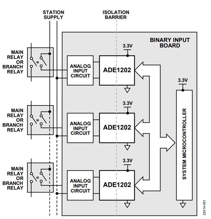
The ADE1202 is a dual-channel, isolated, digital input monitoring solution designed as an interface between mechanical switches and low voltage processors. The ADE1202 communicates the status of the dc input to the system microcontroller as shown in Figure 1. The binary input is designed for 10 V dc to 300 V dc or 8 V rms to 240 V rms ac operation. The system can be configured to support different ranges of analog inputs with the same hardware circuit by changing the system configuration via the ADE1202 register values. This application note describes how to calculate the register values to configure a 300 V dc binary input application.

Application Overview
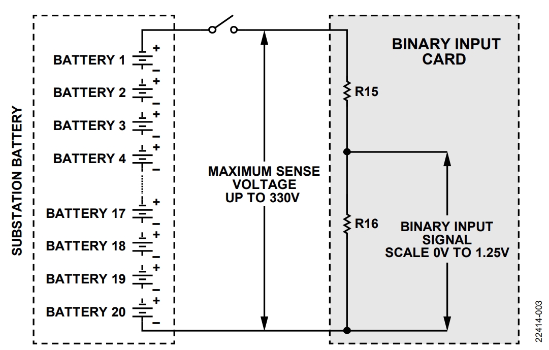
A typical application for the ADE1202 is in substation battery systems where it is necessary to monitor the voltage of the system. The battery voltage during charge can vary ±20% with the voltage reaching as high as 300 V dc or as low as 200 V dc. The recommended application circuit accommodates an extra 10% headroom, which sets the maximum sense voltage, VSENSEMAX, to approximately 330 V dc. The extra headroom captures any over voltage conditions on the battery line. A typical setup of a substation binary input connection is shown in Figure 2.

This application note describes the configuration of the ADE1202 registers to monitor digital inputs, also called binary inputs, to generate a DOUT signal reflecting whether the digital input is a logic high or a logic low. DOUT is typically monitored by a microcontroller or a field-programmable gate array (FPGA). The system software makes decisions based on the state of DOUT
Hardware Considerations
Voltage Divider Selection
The voltage divider scales the substation battery input voltage to 1.25 V, which falls in the input voltage range of the ADE1202. The voltage divider ratio is calculated as follows:
Voltage Divider Ratio = Maximum Input Voltage/VSENSEMAX
= 1.25 V/330 V
= ~0.00378
Selecting values of 285 kΩ for the R15 resistor and 1.1 kΩ for the R16 resistor (see Figure 2) achieves a similar ratio. The ratio of these resistor values results in a voltage divider gain (VGAIN) of 0.003832 . VGAIN sets the maximum measurable voltage at the input of the voltage divider to 326 V dc.
Simplified Schematic
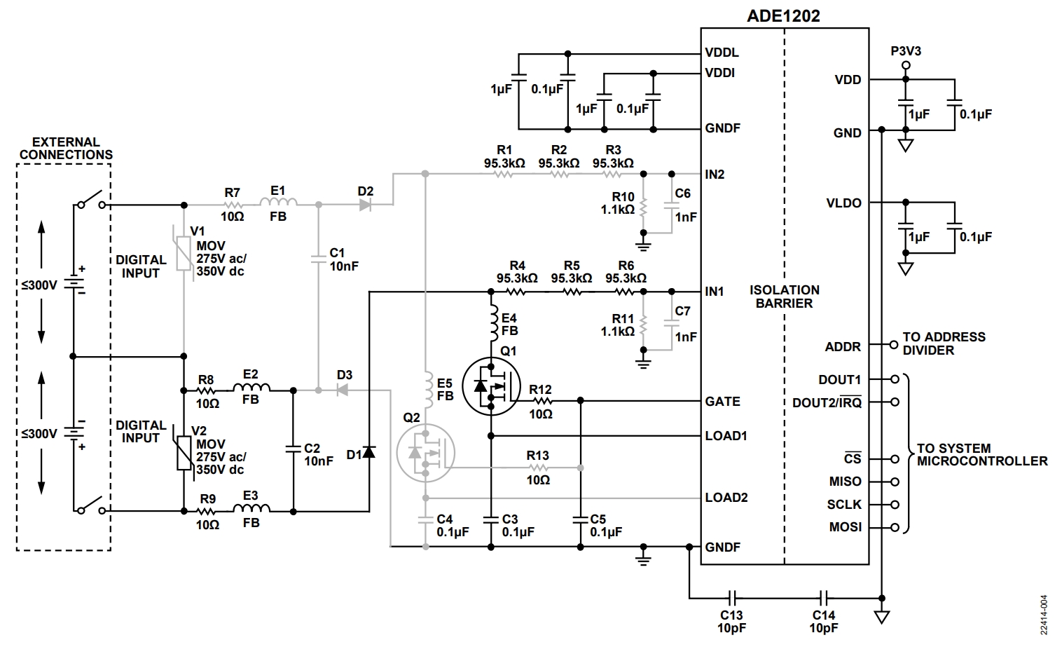
R7, R8, and R9 are current limiting resistors. These resistors limit the current through the system input when there is a high voltage disturbance. The metal-oxide varistor (MOV), V1, clamps the voltage at the input to the binary input card to a predetermined value. The R1, R2, R3, and R10 and R4, R5, R6, and R11 resistors form dividers that allow a maximum voltage of 1.25 V at the IN1 pin or the IN2 pin. Three 95.3 kΩ, 1206 resistors are used, rather than a single 289.3 kΩ resistor, to satisfy the creepage and clearance required to withstand the high voltage levels during a surge or electrostatic discharge (ESD) test, or during a lightning strike. R12 and R13 are current limiting resistors at the gate pins of the metal-oxide semiconductor field effect transistors (MOSFETs). The C1 and C2 capacitors filter out high frequency components of disturbances at the input of the system.
Selecting a MOSFET
The MOSFET serves as a pass device for the programmed load current. The safe operating area (SOA) of the MOSFET must be derated to the maximum operating temperature the circuit is designed for. Derating the SOA allows proper operation of the circuit and prevents the thermal breakdown of the MOSFET. The MOSFET must be rated for the maximum input voltage, the pulse current amplitude, the pulse duration, and the duty cycle. At the highest operating temperature, the operating point of the MOSFET must be within the derated SOA.
The MOSFET on the EVAL-ADE1202EBZ is the SIHFRC20TR-GE3 and has a maximum drain source voltage (VDS) of 600 V and has the current carrying capability suitable for most applications, which allows the MOSFET to withstand high voltage disturbances.

Register Configuration
This section works through an example that sets up the ADE1202 using the configuration shown in Table 1.
| Register | Address | Data |
| CTRL | 0x001 | 0x1040 |
| BIN_CTRL | 0x002 | 0x3610 |
| BIN_THR | 0x003 | 0x5AAA |
| WARNA_THR | 0x004 | 0xCCCC |
| WARNB_THR | 0x005 | 0x5A88 |
| WARNC_THR | 0x006 | 0x2D2D |
| BIN_FILTER | 0x007 | 0x8096 |
| WARNA_FILTER | 0x008 | 0x80FA |
| WARNB_FILTER | 0x009 | 0x80FA |
| WARNC_FILTER | 0x00A | 0x80FA |
| PL_CTRL | 0x010 | 0x0000 |
| PL_RISE_THR | 0x011 | 0x001E |
| PL_LOW_CODE | 0x012 | 0x001E |
| PL_HIGH_CODE | 0x013 | 0x0050 |
| PL_HIGH_TIME | 0x014 | 0x012C |
| EGY_MTR_CTRL | 0x015 | 0x0505 |
| EGY_MTR_THR | 0x016 | 0x01CB |
| PL_EN | 0x200 | 0xC000 |
| PGA_GAIN | 0x201 | 0x0000 |
Identifying Programmable Gain
The ADE1202 has a programmable gain amplifier (PGA) that allows the user to scale the input signal to utilize the full dynamic range of the analog-to-digital converter (ADC). This example uses a PGA gain of 1 and a VGAIN of 0.003832.
Identifying Threshold Codes
The warning and binary channel threshold settings described in Table 2 are the default values. The corresponding threshold voltages based on system assumptions of the PGA gain of 1 and VSENSEMAX of 326 V are as shown in Table 2. Refer to the ADE1202 data sheet for details on how to convert the thresholds to their corresponding register values.
| Register | Threshold Voltage (V) | Threshold Code (Hex) | ||
| High | Low | High | Low | |
| BIN_THR | 217 | 115 | AA | 5A |
| WARNA_THR | 261 | 261 | CC | CC |
| WARNB_THR | 174 | 11 | 88 | 5A |
| WARNC_THR | 58 | 58 | 2D | 2D |
Identifying Filter Codes
For this binary input application, 3 ms of digital filtering is set for the binary channel corresponding to 0x0096 in the BIN_FILTER register. 5 ms of digital filtering is set for the warning channels corresponding to 0x80FA in the WARNx_FILTER registers.
The binary channel is disabled by default, so the BIN_EN bit of the BIN_FILTER register must be set to 0x1 to enable the channel. In the example, the binary channel and warning filters are enabled. Refer to the ADE1202 data sheet for details on converting filter time to a corresponding register value.
Identifying Current Codes
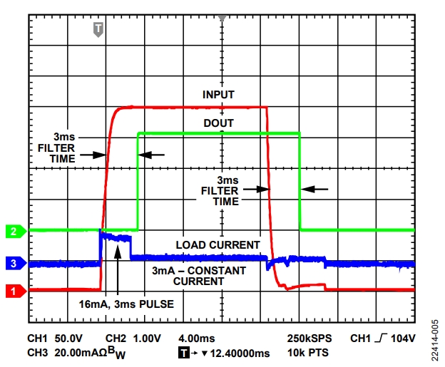
A wetting current dissipates high voltage noise on the line. In this example, the wetting current pulse amplitude is 16 mA and the duration is 3 ms. Therefore, the PL_HIGH_CODE register is set to 0x0050 and the PL_HIGH_TIME register is set to 0x012C, respectively.
The PL_LOW_CODE register is set to 0x001E so that a constant current of 3 mA flows when the pulse ends. Note that the programmable load block is disabled by default. The user must write 0xC000 to the PL_EN register to enable the programmable load block.
The programmable load block has two modes of operation: HIGH_IDLE and LOW_IDLE. In LOW_IDLE mode, the programable load is triggered by a voltage threshold. HIGH_IDLE mode is recommended for effective noise suppression on the binary input channel as high current is applied during the idle state and is not dependent on a voltage threshold. The ADE1202 is set to LOW_IDLE mode by default. The PL_CTRL register default is 0x000.
The threshold used in LOW_IDLE mode is set by the 8-bit register, PL_RISE_THR. In this example, the PL_RISE_THR register is set to 0x001E, which corresponds to 38.4 V. The PL_RISE_THR setting is ignored in HIGH_IDLE mode.
To ensure that a pulsed current is generated when the binary input is high, the following conditions must be observed:
- BIN_FILTER ≥ 0x3
- In LOW_IDLE mode, RISE_THR < BIN_HI_THR

Identifying MOSFET Protection Codes
The combination of high substation voltages and large programmable load currents (up to 51 mA) can destroy the external MOSFET if multiple pulses of large current are applied to the MOSFET in succession.
The ADE1202 can make an accurate estimate of the power being dissipated in the MOSFET. The MOSFET protection is performed using the measured input voltage, or ADC code, and the high current pulse duration to estimate the power generated by the MOSFET over time.
Design Flow and Calculations
Use the following steps to determine the configuration registers that properly configure the MOSFET protection block:
- Derate the MOSFET SOA based on the maximum ambient temperature or case temperature of the MOSFET. Determine the operating VDS, drain current (ID), and safe pulse duration of the derated SOA.
- Calculate the maximum energy threshold and write the value to the EGY_MTR_THR register.
- Set the COOLDOWN_DECR bit and the COOLDOWN_ TIMESTEP bit in the EGY_MTR_CTRL register, based on the MOSFET thermal time constant and the energy threshold.
- Determine the cool down period, which occurs when maximum energy threshold has been exceeded, and set the COOLDOWN_SEC bit of the EGY_MTR_ CTRL register to 0x5.
- Calculate the value that replaces the ADC code when the channel input causes the ADC to overrange. The OV_SCALE bit in the EGY_MTR_CTRL register scales up the instantaneous accumulation adder.
- Write the calculated register values to their corresponding registers.
Refer to the ADE1202 data sheet for the formulas used to calculate each of these register values.
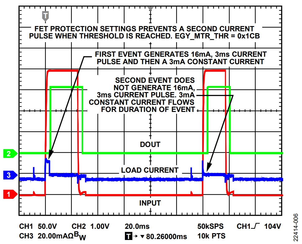
In this example, the energy meter maximum threshold, MAX_EGY_THR, is set to 0x01CB, which is equivalent to the energy dissipated in the MOSFET when the drain voltage is 250 V and the pulse current amplitude is 16 mA for a 3 ms duration. When the calculated threshold is reached, the cool down functionality is triggered, and a cool down period starts (see Figure 5). The duration is specified by the COOLDOWN_SEC bits in the EGY_MTR_CTRL register. The accumulator is zeroed when the device enters the cooldown period. When the pulse current is off, the accumulator is decremented by five counts every 10 µs. By default, the EGY_MTR_CTRL register is set to 0x0505.
When the binary input voltage is large enough, the ADC can hit the full-scale value of 0xFF. When this value is hit, the OV_SCALE bit of the EGY_MTR_CTRL register scales up the instantaneous accumulation adder. The four OV_SCALE factors are 1, 4, 8, and 16.
The EGY_MTR1 or EGY_MTR2 register can be polled for a representation of the accumulated energy in the MOSFET.

ADE1202 Start Up
At power-up, after a hardware reset, or after a software reset, execute the following:
- Poll the INT_STATUS register. The INT_STATUS register reads 0xFFFF during power-up. Upon successful power-up, the RSTDONE bit of the INT_STATUS register reads 0x0000. Write 1 to the RSTDONE bit (Bit 14) of the INT_STATUS register.
- Ensure that the default values are set for the remaining configuration registers.
Note that the binary channel and programmable load are turned off by default. To enable the binary channel and the programmable load circuits, take the following steps:
- Write 0xADE0 to the LOCK_KEY bit of the LOCK register to unlock the device.
- Write new register values to the configuration registers that need to change.
- Write 0xADE1 to LOCK_KEY bit of the LOCK register to lock the device. The ADE1202 is now ready for use.
Author
