AN-1508: Driving the AD9233, AD9246, and AD9254 ADCs in AC-Coupled Baseband Applications
Circuit Function and Benefits
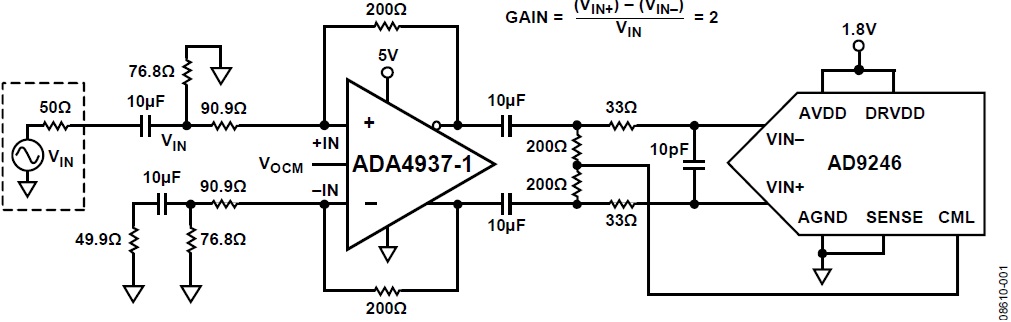
The circuit described in this document and shown in Figure 1 uses the ADA4937-1 ADC driver to convert an ac-coupled, single- ended input signal to a differential signal suitable for driving the AD9246 14-bit, 125 MSPS analog-to-digital converter (ADC). The ADA4937-1 is a low noise, ultralow distortion, high speed differential amplifier with low dc offset and excellent dynamic performance.

It is an ideal choice for driving high performance ADCs with resolutions up to 16 bits from dc to 100 MHz and is suited for a wide variety of data acquisition and signal processing applications. Combined with power and cost savings, this circuit is suitable for applications in communications, instrumentation, and medical imaging. The ADA4937-2 is a dual version of the ADA4937-1 that can be used when driving a dual ADC.
Circuit Description
The AD9246 is a monolithic, 1.8 V single-supply, 14-bit, 80 MSPS/ 105 MSPS/125 MSPS ADC, featuring a high performance sample-and-hold amplifier (SHA) and on-chip voltage reference. The wide bandwidth, truly differential SHA allows a variety of user-selectable input ranges and offsets, including single-ended applications. The device can be applied in multiplexed systems that switch full-scale voltage levels in successive channels and for sampling single-channel input frequencies beyond the Nyquist frequency of the ADC.
The AD9246 achieves its optimum performance when driven differentially. The ADA4937-1 not only provides the single-ended-to-differential conversion but also provides gain and level shifting. The output common voltage of the ADA4937-1 is set by connecting a resistive divider to the VOCM pin of the ADA4937-1. If the pin is left floating, the VOCM voltage is approximately mid supply and set by an internal divider.
The ADA4937-1 is powered with a single 5 V supply and is configured for a gain of 2 for a single-ended, input to differential output. The 76.8 Ω termination resistor, in parallel with the single-ended input impedance of 137 Ω, provides a 50 Ω ac termination for the source. The additional 49.9 Ω resistor, 10 μF capacitor, and 76.8 Ω resistor connected to the 90.9 Ω resistor on the inverting input balance the ac impedance driving the noninverting input. A detailed analysis of this configuration can be found in MT-076 Tutorial.
The signal generator has a symmetric, ground referenced, bipolar output. The VOCM pin of the ADA4937-1 is left unconnected; therefore, the internal divider sets the output common-mode voltage to mid supply. A portion of the voltage is fed back to the summing nodes, biasing the −IN and +IN pins at 1.14 V. For a common-mode voltage of 2.5 V, each ADA4937-1 output swings between 2.0 V and 3.0 V, providing a 2 V p-p differential output for a 1 V p-p single-ended input.
The output of the ADC driver is ac-coupled to a single-pole, low-pass noise filter. The low-pass filter reduces the noise band-width at the ADC input and provides a degree of isolation from the switched capacitor inputs of the ADC and the driver. In any configuration, the optimum value of the shunt capacitor, C, is dependent on the input frequency and source impedance and may need to be optimized. Table 1 displays recommended values for the resistor capacitor (RC) network. These values are dependent on the input signal frequency and can require further optimization.
| Input Frequency Range (MHz) | R Series (Ω) | C Differential (pF) |
| 0 to 70 | 33 | 15 |
| 70 to 200 | 33 | 5 |
| 200 to 300 | 15 | 5 |
| >300 | 15 | Open (no capacitor) |
The input common-mode voltage to the ADC is set by the CML pin of the AD9246 and the pair of 200 Ω resistors. In other applications, the CML pin of the ADC and the VOCM pin of the ADA4937-1 set the input common-mode voltage to the ADC (see the Common Variations section). The ADA4937-1 is fabricated using the Analog Devices, Inc., proprietary silicon germanium (SiGe), complementary bipolar process, enabling it to achieve very low levels of distortion with an input voltage noise of only 2.2 nV/√Hz.
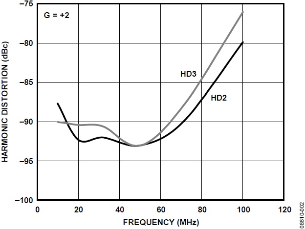
The circuit shown in Figure 1 was tested with a −1 dBFS signal at various input frequencies. Figure 2 shows a plot of the second harmonic distortion (HD2) and third harmonic distortion (HD3) vs. input frequency.

The circuit must be constructed on a multilayer printed circuit board (PCB) with a large area ground plane. Proper layout, grounding, and decoupling techniques must be used to achieve optimum performance (see MT-031 Tutorial, MT-101 Tutorial, and the EVAL-AD9246 evaluation board layout).
To achieve the best electrical and thermal performance, connect the exposed pad on the underside of both the AD9246 and the ADA4937-1 (LFCSP packages) to a large area ground plane. The copper plane must have several vias to achieve the lowest possible resistive thermal path for heat dissipation to flow through the bottom of the PCB. Solder fill or plug these vias.
Common Variations
The AD9246 (14-bit, 80 MSPS/105 MSPS/125 MSPS) ADC is pin compatible with both the AD9233 (12-bit, 80 MSPS/105 MSPS/ 125 MSPS) and the AD9254 (14-bit, 150 MSPS).
There are a few other amplifier configurations to consider when driving ADCs: differential ac-coupled input to differential output, dc-coupled single-ended input to ac-coupled differential output, dc-coupled single-ended input to differential output, and dc-coupled differential input to differential output.
In dc-coupled systems, the driver output common-mode voltage is set via the VOCM pin of the ADA4937-1. The adjustable level of the output common-mode voltage allows the ADA4937-1 output to match the input common-mode voltage of the ADC. The internal common-mode feedback loop of the ADA4937-1 also provides exceptional output balance and suppression of even order harmonic distortion products. Often in these applications, the ADC CML pin is connected directly to the VOCM pin of the driver to ensure that optimal ADC input common-mode voltage is achieved. In other applications, the VOCM pin can be driven from a low impedance source such as an op amp. This pin can also be left floating but bypassed with a capacitor; in this case the VOCM voltage is set at the midpoint of the voltage applied to the two supply pins.
References
MT-074 Tutorial, Differential Drivers for Precision ADCs, Analog Devices.
MT-075 Tutorial, Differential Drivers for High Speed ADCs Overview, Analog Devices.
MT-076 Tutorial, Differential Driver Analysis, Analog Devices.
MT-101 Tutorial, Decoupling Techniques, Analog Devices.
ADI DiffAmpCalc (Differential Amplifier Tool), Analog Devices.