AN-1502: Driving the AD7366/AD7367 Bipolar SAR ADC in Low Distortion DC-Coupled Applications
Circuit Function and Benefits
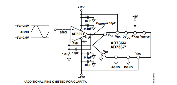
The circuit described in this application note provides single-ended, low-distortion sampling of an industrial level, dc-coupled signal. The driver circuit shown in Figure 1 is optimized for applications requiring best distortion performance. Maximum AD7366/AD7367 performance is achieved by providing adequate settling time and low impedance in the circuit.

Circuit Description
The AD7366 and the AD7367 are, respectively, 12-bit and 14- bit, 1 MSPS, 2-channel, simultaneous sampling successive approximation register (SAR) analog-to-digital converters (ADCs). These devices have a total of four analog multiplexed inputs (two per channel), which operate in single-ended mode. The analog input range on the AD7366/AD7367 is programmable and can support ±10 V, ±5 V, and 0 V to 10 V using the internal 2.5 V reference. An analog input range of ±12 V requires a 3 V external reference.
The AD7366/AD7367 are fabricated on the Analog Devices, Inc., industrial complementary metal-oxide semiconductor (CMOS) process (iCMOS), which is a technology platform combining the advantages of low and high voltage CMOS. The input circuits of the AD7366/AD7367 operate on VDD and VSS voltages of ±12 V, while the rest of the ADC operates on an AVCC, a DVCC, and a VDRIVE of +5 V. The iCMOS process allows the AD7366/AD7367 to accept high voltage bipolar signals in addition to reducing power consumption and package size.
In applications where the signal source has high impedance, it is recommended that the analog input signals be buffered before being applied to the inputs of the AD7366/AD7367, because large source impedances significantly affect the ac performance of the ADC. The choice of the op amp that drives the inputs is a function of the particular application and depends on the analog input voltage range selected. The driver amplifier must be able to settle for a full-scale step to a 14-bit level (0.0061%) for the AD7367 or a 12-bit level (0.024%) for the AD7366 in less than the specified acquisition time of 140 ns.
The AD8021 high performance voltage feedback op amp is an ideal choice as a single-ended input buffer/driver for the AD7366/AD7367 due to its high performance, high speed, low noise, and low distortion performance. Figure 1 shows the configuration of the AD7366/AD7367 with the AD8021 in a single-ended configuration. The AD8021 needs an external compensating NP0 type capacitor (CCOMP), as indicated in Figure 1. The AD8021 is connected in the noninverting mode with a gain of 2. The AD7366/AD7367 programmable bipolar input voltage ranges (referenced to the input of the AD8021) are ±5 V and ±2.5 V.
The circuit must be constructed on a multilayer printed circuit board (PCB) with a large area ground plane. Proper layout, grounding, and decoupling techniques must be used to achieve optimum performance (see the MT-031 Tutorial, the MT-101 Tutorial, and the EVAL-AD7366/EVAL-AD7367 evaluation board layout).
Common Variations
The AD8022 is a suitable replacement for the AD8021 in high frequency applications where a dual version is required. For lower frequency applications, recommended op amps are the AD797, AD845, and AD8610.
References
MT-036 Tutorial, Op Amp Output Phase-Reversal and Input Over-Voltage Protection. Analog Devices.
MT-101 Tutorial, Decoupling Techniques. Analog Devices.