AN-1492: AD5390/AD5391/AD5392 Channel Monitor Function
Circuit Function and Benefits
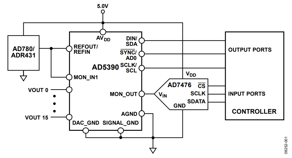
In a multichannel digital-to-analog converter (DAC) system, the ability to monitor all outputs at a single point is a significant advantage for troubleshooting and diagnostic analysis. The circuit shown in Figure 1 provides multichannel DAC output monitoring using a single-channel successive approximation register (SAR) analog-to-digital converter (ADC).

Circuit Description
This circuit utilizes the internal multiplexer on the AD5390/ AD5391/AD5392 to route any of the DAC output channels to a single output pin (MON_OUT) for monitoring by the external ADC (AD7476). This approach utilizes much less circuitry than is required if each channel is monitored individually.
The AD5390/AD5391 are complete, single-supply, 16-channel, 14-bit and 12-bit DACs, respectively. The AD5392 is a complete, single-supply, 8-channel, 14-bit DAC. The devices are available both in 64-lead LFCSP and 52-lead LQFP packages. All channels have an on-chip output amplifier with rail-to-rail operation.
The AD5390/AD5391/AD5392 contain a channel monitor function that consists of a multiplexer addressed via the serial peripheral interface (SPI), allowing any channel output to be routed to the monitor output (MON_OUT) pin for monitoring using an external ADC. The channel monitor function must be enabled in the control register before any channels are routed to the MON_OUT pin. The AD5390/AD5391/AD5392 also include two uncommitted inputs (MON_IN1 and MON_IN2) to the internal multiplexer that allow the user to monitor inputs from external sources such as references or power supplies. In Figure 1, the MON_IN1 pin on the AD5390 monitors the reference voltage from the AD780 and ADR431.
The AD7476 ADC is an SAR ADC that offers 12-bit resolution, single 2.35 V to 5.25 V power supply, integrated reference, low power operation, small form factor, and serial interface, with throughput rates up to 1 MSPS in a 6-lead SOT-23 package. The reference for the device is taken internally from VDD, allowing the widest dynamic input range to the ADC. Therefore, the analog input range for the AD7476 is 0 V to VDD. The conversion rate is determined by the SCLK, allowing throughput rates up to 1 MSPS.
The combination of the AD5390/AD5391/AD5392 and the AD7476 provides a complete 8-channel or 16-channel analog output control solution with an efficient monitor function for system debug, as well as fault and diagnostic analysis.
The AD5390/AD5391/AD5392 and the AD7476 must have ample supply bypassing capacitors of 10 μF in parallel with 0.1 μF capacitors on each supply pin, located as close to the packages as possible, ideally right up against the devices (not shown in Figure 1). The 10 μF capacitors are the tantalum bead type. The 0.1 μF capacitors must have low effective series resistance (ESR) and low effective series inductance (ESL). Common ceramic type capacitors provide a low impedance path to ground at high frequencies to handle transient currents due to internal logic switching.
The power supply traces must be as wide as possible to provide low impedance paths and reduce the effects of glitches on the power supply line. Fast switching signals, such as clocks, must be shielded with ground runs to avoid radiating noise to other parts of the board and must never be run near the analog signals. A ground line routed between the SDATA and SCLK lines helps reduce crosstalk between them (not required on a multilayer board, which has a separate ground plane; however, it is helpful to separate the lines). Avoid crossover of digital and analog signals. Run traces on opposite sides of the board at right angles to each other to reduce the effects of feedthrough on the board. A microstrip technique is recommended but not always possible with a double-sided board. In this technique, the component side of the board is dedicated to the ground plane, and signal traces are placed on the solder side. Best layout and performance is achieved with at least a 4-layer multilayer board, where there is a ground plane layer, a power supply layer, and two signal layers.
Common Variations
Pin-compatible versions of the AD7476 are available for use in applications where lower resolution conversion is acceptable in the monitoring function. The AD7477 provides 10-bit resolution, and the AD7478 provides 8-bit resolution. The ADR431 reference can be substituted for the AD780.
References
Kester, Walt. Chapter 3 and Chapter 7. The Data Conversion Handbook. Analog Devices. 2005.
MT-015 Tutorial. Basic DAC Architectures II: Binary DACs. Analog Devices.