

MAX38801
PRODUCTIONIntegrated, Step-Down Switching Regulator with Selectable Applications Configurations
15A Fully Integrated, Highly Efficient Switching Regulator
- Part Models
- 2
- 1ku List Price
- Starting From $4.56
Overview
- High-Efficiency Solution
- Up to 96% Peak
- Up to 92% Full Load
- Up to 94% Light-Load Efficiency at 1A with DCM Enabled
- Flexible Design Allows Early PCB Definition
- Footprint Compatible with MAX38800 (9A) and MAX38802/MAX38803 (25A)
- Programmable Switching Frequency up to 900kHz
- Programmable Soft-Start and STAT Delay Timings
- Programmable Reference Voltage with External Input Option
- Programmable Positive and Negative OCP Limit
- Advanced Architecture, Protection and Reporting Guarantees Reliable Designs
- Analog Current or Temperature Reporting
- Differential Remote Sense with Open-Circuit Detection
- Fast Transient Response with Quick-PWM™ Architecture
- Percentage-Based Output Power Good and OVP
- Open-Drain Status Indicator (STAT) Pin
- Input Undervoltage and Overvoltage Lockout
- Adaptive Dead-Time Control
- Saves Board Space
- Integrated Boost Switch
- 19-Ball WLCSP (2.2mm x 2.8mm) Footprint
- Operation Using Ceramic Input and Output Capacitors
The MAX38801 is a fully integrated, highly efficient switching regulator for applications operating from 6.5V to 14V input supplies that require up to 15A maximum load. This single-chip regulator provides compact high-efficiency power delivery for precision outputs that demand fast transient response.
The device has different programmability options to enable a wide range of configurations. The programmable features include: internal/external reference voltage, output voltage set-point, switching frequency, overcurrent-protection level (OCP), and soft-start timing. Discontinuous current mode (DCM) operation can be enabled using pinstrapping to improve light-load efficiency.
The MAX38801 includes multiple protection and measurement features. Positive and negative cycle-by-cycle OCP, short-circuit protection and overtemperature protection (OTP) ensure robust design. Input undervoltage and overvoltage lockout shut down the regulator to prevent damages when the input voltage is out of specification. Regulation is halted in case of an output overvoltage (OVP) event. A status pin indicates that the output voltage is within range and the output voltage is in regulation. The device has an analog output that can be configured to report output current or junction temperature with ±5% and ±8°C accuracy, respectively.
Applications
- DDR Memory: VDDQ, VPP and VTT
- GPU Core Supply
- I/O and Chipset Supplies
- Point-of-Load (POL) applications
- Servers/μServers
Documentation
Data Sheet 1
Evaluation Design File 1
ADI has always placed the highest emphasis on delivering products that meet the maximum levels of quality and reliability. We achieve this by incorporating quality and reliability checks in every scope of product and process design, and in the manufacturing process as well. "Zero defects" for shipped products is always our goal. View our quality and reliability program and certifications for more information.
| Part Model | Pin/Package Drawing | Documentation | CAD Symbols, Footprints, and 3D Models |
|---|---|---|---|
| MAX38801HCS+ | WLCSP | ||
| MAX38801HCS+T | WLCSP |
| Part Models | Product Lifecycle | PCN |
|---|---|---|
|
Apr 24, 2020 - 2051 MECHANICAL DATASHEET |
||
| MAX38801HCS+ | PRODUCTION | |
This is the most up-to-date revision of the Data Sheet.
Software Resources
Can't find the software or driver you need?
Request a Driver/SoftwareTools & Simulations
ADI Power Studio™ Designer
ADI Power Studio™ Designer is the next-generation tool for IC-level, power supply design, guiding engineers to faster, validated solutions.
Learn MoreSIMPLIS Models 1
Evaluation Kits
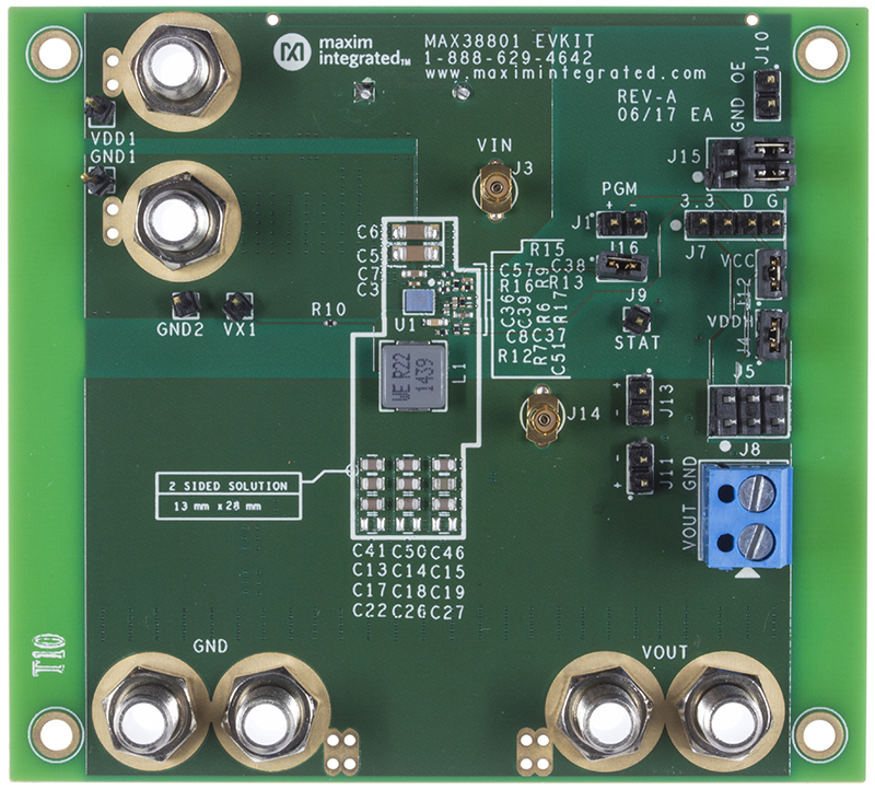
Evaluation Kit for the MAX38801
Resources
Latest Discussions
No discussions on MAX38801 yet. Have something to say?
Start a Discussion on EngineerZone®