

MAX16712
PRODUCTIONDual-Output, 6A, 2MHz, 2.7V to 16V Step-Down Switching Regulator
Shrink Your Designs with Smallest and Fastest Two Regulators in One Package
- Part Models
- 2
- 1ku List Price
- Starting From $2.94
Overview
- High Power Density with Low Component Count
- Dual-Output or Dual-Phase Operation
- Single-Supply Operation with Integrated LDO for Bias Generation
- Compact 2.2mm x 3.5mm, 28-Bump WLP
- Internal Compensation
- Wide Operating Range
- 2.7V to 16V Input Voltage Range
- 0.5V to 5.8V Output Voltage Range
- 500kHz to 2MHz Configurable Switching Frequency
- -40°C to +125°C Junction Temperature Range
- Three Programming Pins to Select Different Configurations
- Independent Enable and Power Good for Each Output
- Optimized Performance and Efficiency
- 90.5% Peak Efficiency with VDDH = 12V, VOUT = 1.8V, and fSW = 1MHz
- Interleaved 180° Out-of-Phase Operation
- AMS to Improve Load Transient
- Selectable DCM to Improve Light Load Efficiency
- Active Current Balancing for Dual-Phase Operation
The MAX16712 is a dual-output, fully integrated, highly efficient, step-down DC-DC switching regulator. The device operates from 2.7V to 16V input supplies, and each output can be regulated from 0.5V to 5.8V. The IC delivers up to 6A of load current per output. The two outputs can be connected in parallel as a single-output, dual-phase regulator that supports up to 12A load current.
The switching frequency of the device can be configured from 500kHz to 2.0MHz and provides the capability of optimizing the design in terms of solution size and performance.
The MAX16712 utilizes fixed-frequency, current-mode control with internal compensation. The dual-switching regulators operate 180° out-of-phase. The IC features an advanced modulation scheme (AMS) and selectable discontinuous current mode (DCM) operation to provide improved performance. Operation settings and configurable features can also be selected by connecting a pin-strap resistor from PGM0 pin to ground.
The MAX16712 has an internal 1.8V LDO output to power the gate drives (VCC) and internal circuitry (AVDD).
The MAX16712 integrates multiple protections including positive and negative overcurrent protection, output overvoltage protection and overtemperature protection to ensure robust design.
The device is available in a compact 2.2mm x 3.5mm wafer-level package (WLP). It supports -40°C to +125°C junction temperature operation.
Applications
- Communications Equipment
- I/O Pins of an FPGA/DSP/MCU
- Memory VDDQ
- Networking Equipment
- Point-of-Load (POL) Voltage Regulators
- Servers and Storage Equipment
- μP Chipsets
Documentation
Data Sheet 1
Video 1

ADI has always placed the highest emphasis on delivering products that meet the maximum levels of quality and reliability. We achieve this by incorporating quality and reliability checks in every scope of product and process design, and in the manufacturing process as well. "Zero defects" for shipped products is always our goal. View our quality and reliability program and certifications for more information.
| Part Model | Pin/Package Drawing | Documentation | CAD Symbols, Footprints, and 3D Models |
|---|---|---|---|
| MAX16712AWI+ | WLCSP | ||
| MAX16712AWI+T | WLCSP |
This is the most up-to-date revision of the Data Sheet.
Software Resources
Can't find the software or driver you need?
Request a Driver/SoftwareTools & Simulations
ADI Power Studio™ Designer
ADI Power Studio™ Designer is the next-generation tool for IC-level, power supply design, guiding engineers to faster, validated solutions.
Learn MoreSIMPLIS Models 1
Evaluation Kits
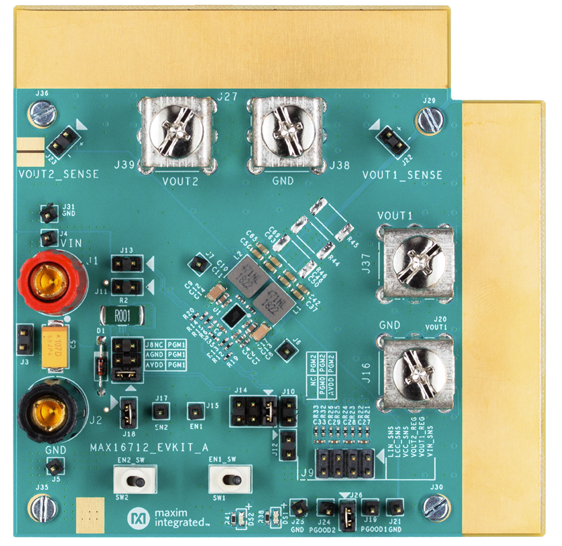
Evaluation Kit for the MAX16712
Resources
Latest Discussions
No discussions on MAX16712 yet. Have something to say?
Start a Discussion on EngineerZone®