

ADP5053
PRODUCTIONIntegrated Power Solution with Quad Buck Regulators and Supervisory Circuits
- Part Models
- 1
- 1ku List Price
- Starting From $6.16
Overview
- Wide input voltage range: 4.5 V to 15.0 V
- ±1.5% output accuracy over full temperature range
- 250 kHz to 1.4 MHz adjustable switching frequency
- Adjustable/fixed output options via factory fuse
- Power regulation
- Channel 1 and Channel 2: programmable 1.2 A/2.5 A/4 A sync buck regulators with low-side FET driver
- Channel 3 and Channel 4: 1.2 A sync buck regulators
- Single 8 A output (Channel 1 and Channel 2 operated in parallel)
- Precision enable with 0.8 V accurate threshold
- Active output discharge switch
- FPWM or automatic PWM/PSM selection
- Frequency synchronization input or output
- Optional latch-off protection on OVP/OCP failure
- Power-good flag on selected channels
- UVLO, OCP, and TSD protection
- Open-drain processor reset with external adjustable threshold monitoring
- Watchdog refresh input
- Manual reset input
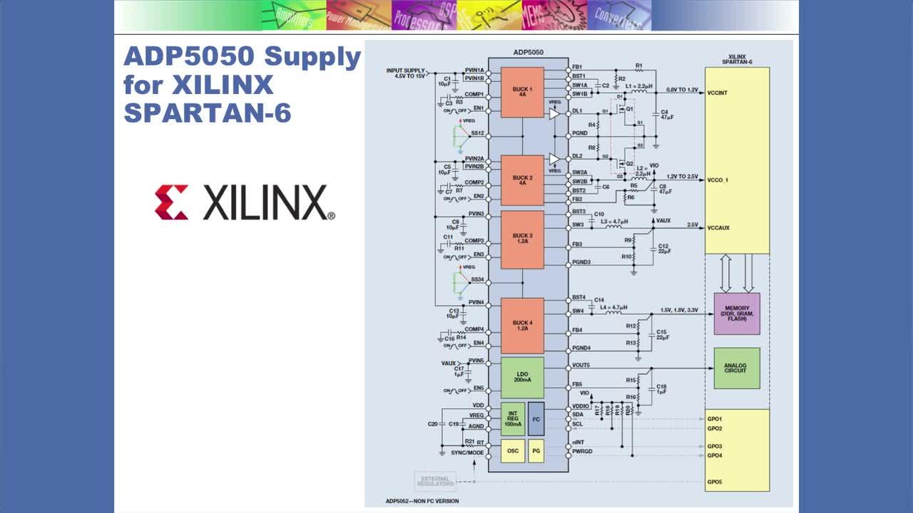
The ADP5053 combines four high performance buck regulators, a supervisory circuit, a watchdog timer, and a manual reset in a 48-lead LFCSP package that meets demanding performance and board space requirements. The device enables direct connection to high input voltages up to 15.0 V with no preregulators.
Channel 1 and Channel 2 integrate high-side power MOSFET and low-side MOSFET drivers. External NFETs can be used in low-side power devices to achieve an efficiency optimized solution and deliver a programmable output current of 1.2 A, 2.5 A, or 4 A. Combining Channel 1 and Channel 2 in a parallel configuration can provide a single output with up to 8 A of current.
Channel 3 and Channel 4 integrate both high-side and low-side MOSFETs to deliver an output current of 1.2 A.
The switching frequency of the ADP5053 can be programmed or synchronized to an external clock. The ADP5053 contains a precision enable pin on each channel for easy power-up sequencing or adjustable UVLO threshold.
The ADP5053 contains supervisory circuits that monitor the voltage level. The watchdog timer can generate a reset if the WDI pin is not toggled within a preset timeout period. Processor reset mode or system power on/off switch mode can be selected for manual reset functionality.
Applications
- Small cell base stations
- FPGA and processor applications
- Security and surveillance
- Medical applications
Documentation
Data Sheet 1
Video 1
Brochure 1
Analog Dialogue 1
ADI has always placed the highest emphasis on delivering products that meet the maximum levels of quality and reliability. We achieve this by incorporating quality and reliability checks in every scope of product and process design, and in the manufacturing process as well. "Zero defects" for shipped products is always our goal. View our quality and reliability program and certifications for more information.
| Part Model | Pin/Package Drawing | Documentation | CAD Symbols, Footprints, and 3D Models |
|---|---|---|---|
| ADP5053ACPZ-R7 | 48-Lead LFCSP (7mm x 7mm x 0.75mm w/ EP) |
| Part Models | Product Lifecycle | PCN |
|---|---|---|
|
Aug 6, 2014 - 14_0135 Assembly and Test Transfer of AD7173-8, AD7175-8 in 6x6 mm and ADP5051, ADP5053 in 7x7 mm LFCSP to StatsChipPac China |
||
| ADP5053ACPZ-R7 | PRODUCTION | |
|
Nov 12, 2013 - 13_0232 Assembly and Test Transfer of Select 6x6 and 7x7mm LFCSP Products to STATS ChipPAC China |
||
| ADP5053ACPZ-R7 | PRODUCTION | |
This is the most up-to-date revision of the Data Sheet.
Software Resources
Can't find the software or driver you need?
Request a Driver/SoftwareTools & Simulations
LTspice
Models for the following parts are available in LTspice:
- ADP5053
ADP505x Buck Regulator Design Tool
Microsoft Excel download tool from ADIsimPower to generate a power supply design complete with a schematic, bill of materials, and performance specifications.
Open ToolLTspice® is a powerful, fast and free simulation software, schematic capture and waveform viewer with enhancements and models for improving the simulation of analog circuits.
Evaluation Kits
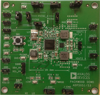
ADP5053 Evaluation Board
Resources
ADP5053 Evaluation Board