

ADP5140
PRE-RELEASEPower Management IC for Automotive Application
- Part Models
- 1
- 1ku List Price
- Starting From $8.42
Overview
- Buck regulators
- BUCK1, 2.5 A maximum continuous output current range with DVS
- BUCK2, 2.5 A maximum continuous output current range with adjustable output voltage
- BUCK3, 3 A maximum continuous output current range with adjustable output voltage
- BUCK4, 3 A maximum continuous output current range with low noise output
- Boost regulator: fixed 5 V output, 400 mA output current range
- Seven LDO regulators with low noise output
- LDO1: 300 mA
- LDO2: 2.3 A
- LDO3: 1.4 A
- LDO4: 1.2 A
- LDO5: 500 mA
- LDO6: 50 mA
- LDO7: 400 mA
- 2.2 MHz (typical) switching frequency
- Synchronization input or output
- Out of phase between buck regulators
- Integrated soft start and compensation for all regulators
- Overcurrent and thermal protection for all power rails
- 2 window voltage monitors
- 2 window watchdogs with pulse detection
- One QA watchdog
- Wake-up input
- SPI for control and diagnostics
- RESET, FAULT, and STATUS outputs
- 56-terminal LGA
- AEC-Q100 qualified for automotive applications
The ADP5140 integrates four high performance, synchronous, step-down buck regulators (BUCK1 to BUCK4), one boost regulator, and seven low noise, low dropout (LDO) regulators (LDO1 to LDO7). The buck regulators support input voltages from 2.7 V to 5.5 V and provide output currents from 2.5 A to 3 A. The boost regulator provides a fixed 5 V output and provides a 400 mA load current. The seven LDOs provide a clean output voltage for the system. LDO5 provides an ultralow noise output that can be used to power noise sensitive loads.
The ADP5140 runs in a fixed 2.2 MHz switching frequency (fSW) or can synchronize to an external clock from its 1.9 MHz to 2.4 MHz synchronization range, which is outside of the amplitude modulation (AM) band. The four buck regulators run at 90° out of phase to reduce the input ripple current and the input capacitor size, which lowers the system electromagnetic interference (EMI).
All regulators integrate internal compensation to simplify the design. The internal soft start circuitry and power-up sequencing reduce the input inrush current.
Each voltage rail is monitored internally and any fault event is reported to the system through the RESET, FAULT, and STATUS pins. Two window watchdogs (WD0 and WD1) and one question answer (QA) watchdog monitor the processor or other devices in the system to ensure that any software or hardware errors are detected. The ADP5140 integrates a serial peripheral interface (SPI) for system control and diagnostics.
Additional protection includes current-limit protection, overvoltage protection, undervoltage protection, and thermal shutdown (TSD).
The ADP5140 operates over a junction temperature range of −40°C to +150°C and is available in a 56-terminal, land grid array (LGA).
APPLICATIONS
- Advanced driver assistance (ADAS)
- Automotive electronics
- Infotainment system
- Industrial and instrumentation
Documentation
Data Sheet 1
User Guide 1
ADI has always placed the highest emphasis on delivering products that meet the maximum levels of quality and reliability. We achieve this by incorporating quality and reliability checks in every scope of product and process design, and in the manufacturing process as well. "Zero defects" for shipped products is always our goal. View our quality and reliability program and certifications for more information.
| Part Model | Pin/Package Drawing | Documentation | CAD Symbols, Footprints, and 3D Models |
|---|---|---|---|
| ADP5140WACCZ-R7 | 56-Terminal Land Grid Array [LGA] (8mm x 8mm x 0.864 m) |
This is the most up-to-date revision of the Data Sheet.
Software Resources
Can't find the software or driver you need?
Request a Driver/SoftwareEvaluation Kits
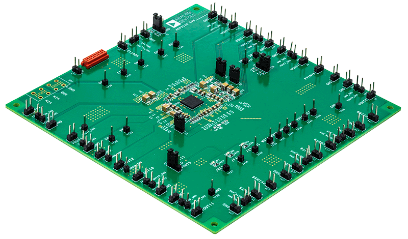
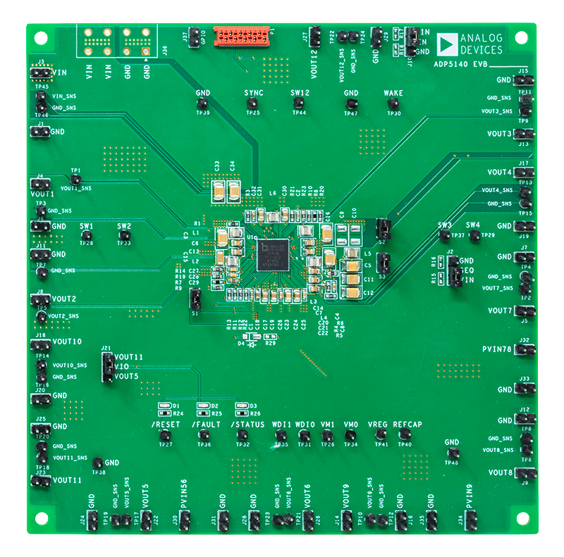
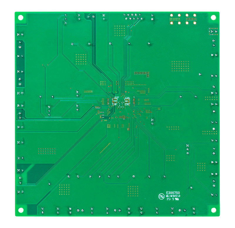
Evaluating the ADP5140 Power Management IC for Automotive Application
Resources
Latest Discussions
No discussions on ADP5140 yet. Have something to say?
Start a Discussion on EngineerZone®