AD4858
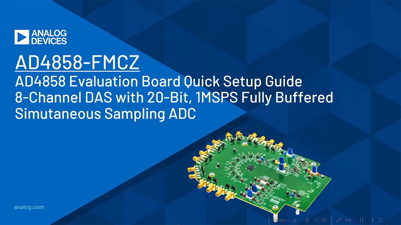
RECOMMENDED FOR NEW DESIGNSBuffered, 8-Channel Simultaneous Sampling, 20-Bit 1 MSPS DAS
- Part Models
- 2
- 1ku List Price
- Starting From $51.72
Overview
- Complete 20-bit data acquisition system
- Simultaneous sampling of 8 internally buffered channels
- 1 MSPS per channel throughput
- Differential, wide common-mode range inputs
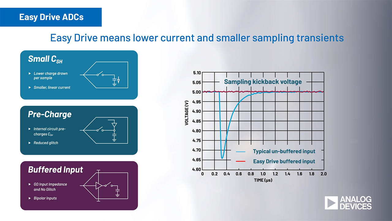
- ±75 pA typical input leakage at 25°C
- Full-scale input step settling time < 300 ns
- Integrated reference and reference buffer (4.096 V)
- Integrated supply decoupling capacitors
- 45 mW per channel at 1 MSPS, power scales with throughput
- Minimal external signal conditioning
- Seamless high dynamic range
- Per sample, per channel automatic gain ranging
- Maintains ppm-level INL
- Per channel SoftSpan input ranges, bipolar or unipolar
- ±40 V, ±25 V, ±20 V, ±12.5 V, ±10 V, ±6.25 V, ±5 V, ±2.5 V
- 0 V to 40 V, 25 V, 20 V, 12.5 V, 10 V, 6.25 V, 5 V, 2.5 V
- Rail-to-rail input overdrive tolerance
- High performance
- INL: ±160 μV typical (±40 V range)
- SNR: 97.2 dB single-conversion typical (±40 V range)
- DR: 111.4 dB single-conversion typical (±40 V range)
- THD: −117 dB typical (±40 V range)
- CMRR: 120 dB typical
- Digital flexibility
- SPI CMOS (0.9 V to 5.25 V) and LVDS serial input and output
- Optional oversampling with 24-bit digital averaging
- Optional offset, gain and phase correction
- 7.00 mm × 7.00 mm, 64-ball BGA full solution footprint
The AD4858 is a fully buffered, 8-channel simultaneous sampling, 20-bit, 1 MSPS data acquisition system (DAS) with differential, wide common-mode range inputs. Its functional architecture is shown in Figure 1 in the data sheet. Operating from a 5 V low voltage supply, flexible input buffer supplies, and using the precision low drift internal reference and reference buffer, the AD4858 allows the SoftSpan range of each channel to be independently configured to match the native application signal swing, minimizing additional external signal conditioning. To further maximize single-conversion dynamic range, the AD4858 incorporates seamless high dynamic range (SHDR) technology. When enabled, the input signal path gain of the channel is automatically optimized on a sample-by-sample basis, minimizing converter noise on each sample without impacting linearity.
The 11 MHz bandwidth, picoamp input analog buffers, wide input common-mode range, and 120 dB common-mode rejection ratio (CMRR) of the AD4858 allow the DAS to directly digitize input signals with arbitrary swings on INx+ and INx−. Its input signal flexibility, combined with ±160 μV integral nonlinearity (INL), no missing codes at 20 bits, 97.2 dB signal to noise ratio (SNR), and 111.4 dB dynamic range (DR), make the AD4858 an ideal choice for applications requiring high accuracy, throughput, and precision in a compact solution footprint. Enabling 24-bit oversampling offers further SNR and dynamic range improvements. Optional per channel offset, gain, and phase adjustment provide the ability to calibrate and remove system-level errors upstream to the DAS.
The AD4858 features a serial peripheral interface (SPI) register configuration bus (0.9 V to 5.25 V), and supports both low voltage differential signaling buses (LVDS) and complementary metal-oxidize semiconductor (CMOS) conversion data output buses, selectable using the LVDS/CMOS pin. Between one and eight lines of data output can be employed in CMOS mode, allowing the user to optimize bus width and throughput.
The 7.00 mm × 7.00 mm, 64-ball, ball grid array (BGA) of the AD4858 includes all critical power supply and reference bypass capacitors, minimizing full solution footprint and component count, and reducing sensitivity to application printed circuit board (PCB) layout. It operates over an extended industrial temperature range of −40°C to +125°C.
APPLICATIONS
- Automatic test equipment
- Avionics and aerospace
- Instrumentation and control systems
- Semiconductor manufacturing
- Test and measurement
Documentation
Data Sheet 1
User Guide 1
Video 3
Device Drivers 1
ADI has always placed the highest emphasis on delivering products that meet the maximum levels of quality and reliability. We achieve this by incorporating quality and reliability checks in every scope of product and process design, and in the manufacturing process as well. "Zero defects" for shipped products is always our goal. View our quality and reliability program and certifications for more information.
| Part Model | Pin/Package Drawing | Documentation | CAD Symbols, Footprints, and 3D Models |
|---|---|---|---|
| AD4858BBCZ | 64-Lead BGA (7 mm x 7 mm x 1.42 mm) | ||
| AD4858BBCZ-RL-13 | 64-Lead BGA (7 mm x 7 mm x 1.42 mm) |
This is the most up-to-date revision of the Data Sheet.
Software Resources
Device Drivers 1
Evaluation Software 2
Precision Toolbox for MATLAB
The Precision Toolbox is an evaluation software, made available in MATLAB, that allows configuring and capturing data with ADI’s precision data converters. To get started evaluating with the Precision Toolbox:
Step 1: Setup the evaluation hardware as described in the hardware setup guide.
Step 2: Install the Precision Toolbox and its dependencies. Refer to the Precision Toolbox wiki.
Software Drivers
Can't find the software or driver you need?
Hardware Ecosystem
| Parts | Product Life Cycle | Description |
|---|---|---|
| LDO Linear Regulators 3 | ||
| LT1761 | RECOMMENDED FOR NEW DESIGNS | 100mA, Low Noise, LDO Micropower Regulators in TSOT-23 |
| ADP150 | PRODUCTION | Ultralow Noise, 150 mA CMOS Linear Regulator |
| ADP151 | PRODUCTION | Ultralow Noise, 200 mA, CMOS Linear Regulator |
| Switching Regulators & Controllers 2 | ||
| LT8330 | RECOMMENDED FOR NEW DESIGNS | Low IQ Boost/SEPIC/Inverting Converter with 1A, 60V Switch |
| ADP5070 | PRODUCTION | 1 A/0.6 A, DC-to-DC Switching Regulator with Independent Positive and Negative Outputs |
| Voltage References 2 | ||
| LTC6655 | PRODUCTION | 0.25ppm Noise, Low Drift Precision References |
| ADR4540 | PRODUCTION | Ultra-Low-Noise, High-Accuracy 4.096V Voltage Reference |
Tools & Simulations
LTspice 1
Models for the following parts are available in LTspice:
- AD4858
Design Tool 1
Signal Chain Designer
Signal Chain Designer is a web-based tool designed to create and simulate complex precision signal chains. See your circuit’s performance before you commit to your PCB: transfer function, noise, power consumption, input range, and DC error. Quickly experiment with different parts and architectures. Signal chains can be exported to LTspice for further analysis.
Open ToolIBIS Model 1
LTspice® is a powerful, fast and free simulation software, schematic capture and waveform viewer with enhancements and models for improving the simulation of analog circuits.


