Selecting the Right N-Channel MOSFET for the MAX14922 for High-Side Industrial Output Applications
摘要
This application note explains how to select the right external n-channel MOSFET used with the MAX14922 in high-side industrial load switch applications.
Introduction
High-side switches commonly control industrial loads and are usually known as digital output devices. Industrial digital output loads are generally inductive in nature. The high-side switches are used in applications such as drive control of lamps, controlling relays, and driving actuator loads/solenoids. Turning the loads on or off as fast as possible enables efficient power utilization. However, it also creates unwanted voltage spikes, which is detrimental to the switch and controller if the components are not selected correctly.
The MAX14922 is a simple and effective way to control and drive an external n-channel MOSFET device, reducing component count, yet providing the efficient and reliable performance needed for industrial and safety applications.
This application note explains how to select the right external n-channel MOSFET and pick the right protection based on the application needs.
MAX14922 in a High-Side Industrial Output Application
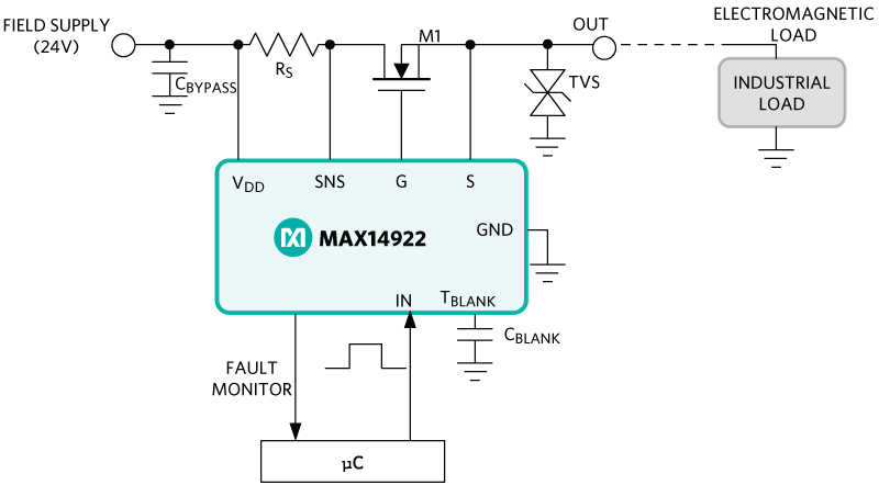
Figure 1. The MAX14922 with an external FET driving a typical digital output load/actuator.
The typical high-side switch application with the MAX14922 has the following vital components:
- External power FET (nMOS)
- Protection diodes TVS (at the source terminal)
- Optional protection diodes at the VDD or system power input
- CBLANK capacitance to auto-retry in fault/overcurrent conditions
Figure 1 shows a simplified application circuit with the MAX14922 connecting the system power input to a typical industrial load. The electromagnetic load operates by consuming power from the input to convert electrical to mechanical energy. The requirements of the application dictate the power handling capabilities of the load, which determines the system operating current.
Benefits of the MAX14922
A MAX14922-based high-side switch circuit offers the following key benefits:
- The MAX14922 is suitable for applications with typical 24V DC power, as well as those working up to 70V high-voltage industrial supplies.
- High currents are possible as defined by the n-channel MOSFET (M1).
- Ultra-low RDSON switch resistance is achievable as defined by the n-channel MOSFET.
- High inductive energy switching and clamping as defined by the external GND-connected TVS.
- Supply-voltage independent inductive load turn-off or demagnetization times, as the TVS clamp is GND-connected.
- Supports very fast inductive load turn-off: the MAX14922 allows very high inductive clamping voltages of up to -70V at output (at source).
- Monitoring of the switch output through the integrated comparator.
Selecting the Right N-Channel Power FET
The application dictates the working voltage and current, which is determined from the load demand of the load/actuator. It is prudent to choose the external FET with the lowest RDSON. This enables efficient power delivery from the source to the load. The total drop across the high-side switch function is:

where RS is the resistance of the sense resistor. Keeping the channel on-resistance RDSON to a minimum ensures lower power dissipation.
The n-channel FET's maximum drain-source voltage (VDSS) or VBR must be equal to or greater than the VCLAMP voltage + VDD. The VCLAMP is the negative clamped voltage during surge or load turn-off, which is determined by the TVS clamp voltage. See the sections on inductive demagnetization and surge protection for more information. The MOSFET's threshold voltage (VTH) must be greater than 0.8V and able to handle VGS voltages up to 16V. The normal functional load current and the fault currents in the application must be within the Safe Operating Area (SOA) of the n-channel FET. The SOA is temperature dependent. So, the FET must be temperature derated to the desired operating temperature to ensure the switch is within the nominal operating conditions.
Blanking Time and Auto Retry During Over-Current Events
Miswiring errors during installation or maintenance, load wear/tear over time, or sudden damage to the actuator are the typical reasons for load failures. The series sensing resistor RS, MAX14922, and external FET work together to regulate the set current for a period in cases of over-current faults or short circuits. Then the FET is forced off if the over-current scenario persists, only for it to turn back on after the auto-retry time. This way, the switch/power supply and component blocks are protected, and the fault condition is relayed over to the system controller to intervene.
Shorting the tBLANK input to the ground enables a continuous maximum set current regulated output during over-current events if the blanking time and auto-retry mode are not preferred. Care must be taken during such instances as the external FET is forced to be in the resistive or linear mode, which increases the power dissipation. The FET is damaged when the continuous power dissipation is more than the n-channel FET's thermal dissipation specification, hence compromising the application.
The SOA curve of the selected FET, for example for Si7322DN (Figure 2), provides critical information on the maximum drain current it can handle as a function of VDS and with the duration. The drain current here is associated with the maximum RS current limit.
Figure 2 shows that for a given VDS (maximum supply voltage at the load, which is VDD) as the load current increases along the y-axis, its on-time decreases on the second y-axis to the right. This information is used to determine the appropriate CBLANK capacitance, which sets the blanking time and auto-retry function to ensure the FET is kept within the safe operating area. More information about derating the SOA over temperature can be found in the reference link (derating of the MOSFET safe operating area - Toshiba).
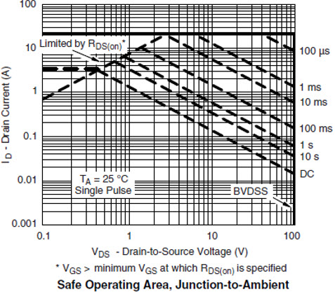
Figure 2. SOA of the Si7322DN. Courtesy TOC from the Si7322DN data sheet.
Inductive Demagnetization
The MAX14922 turns the external switch (FET) on or off, which either delivers power or cuts off power to the load. If the load is inductive or connected with long cables that generate inductance along the load line. Abruptly turning off the power generates unwanted back EMFs, where the energy stored at the inductive load must be dissipated safely back to the power return path. External TVS protection is required for inductive load demagnetization at the source of the FET to dissipate the energy safely. The TVS limits the negative voltage excursion at the source terminal to keep the VDS of the FET lower than the VDSS. The energy stored in the load inductance (EL) is defined as:

where ILOAD is the working load current.
A TVS diode at source input (Figure 3) dissipates the back electromagnetic interference (EMF) generated by load in tDEMAG seconds as:

where VDD is the application power supply input at the drain of the FET.
VCLAMP is the TVS clamping voltage to protect from negative overvoltage.
R is the equivalent resistance of the load (VDD/ILOAD)
The load inductance (L) and the effective DC resistance (R) are parameters based on the load. The higher the VCLAMP voltage, the faster the TVS takes (time = tDEMAG) to dissipate the stored energy. The FET's VDSS must be greater or equal to VCLAMP + VDD of the application.
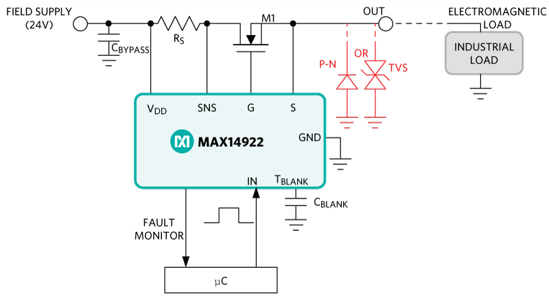
Figure 3. Typical 24V application diagram with TVS or PN diode at S.
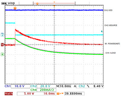
Figure 4a. Slow tDEMAG when using a PN diode with 320mA and 1H inductance, and 75? resistance.
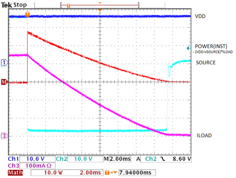
Figure 4b. Fast tDEMAG when using a TVS diode with 450mA and 1.5H inductance.
Figure 4a shows demagnetization waveforms when a diode is used for clamping the inductive energy. The diode's low forward voltage at -0.3V typical results in very long demagnetization times of 60ms.
Figure 4b shows a demagnetization curve when using a SMB33CA TVS, which clamps at -37V resulting in faster demagnetization of 16ms, even with a 40% higher initial load current.
The choice of protection affects how fast the load can be switched off and the choice of PN diode impedes the switching rate of the inductive load.
As the high-side switch switching rates are increased, the power dissipation increases proportionally in the clamp. The inductive clamp must be selected to allow dissipation of the power dissipation during the highest switching rates.
The inductor discharge current during demagnetization (Figure 4b) can be approximated to a linear model to calculate the peak and average energy dissipated from the TVS. The area under the triangle (Figure 4b) of discharge current across the clamp for 17ms provides the average energy across the clamp.
Peak power across the clamp = ILOAD (A) x (|VCLAMP|V)
and the energy dissipated by the clamp during the demagnetization event is:
ECLAMP = 0.5 x ILOAD (A) x (|VCLAMP|V) x tDEMAG
Surge Protection for the Application: Selecting the Right TVS
The surge level requirements are defined by the end equipment manufacturer, and it is critical the system can handle protection for these levels. Typically, digital outputs (DO) have specified surge limits with a 42? tester source impedance characteristic. Table 1 shows the peak current observed at the source terminal of MAX14922 for specific surge levels.
The TVS must be chosen based on its capability to handle peak currents within the rated peak current in the TVS data sheet (8µs/20µs current waveform during short based on IEC 61000-4-5).
| Surge Level (KV) | Surge Resistance | Peak Surge Current at S (A) |
| ±0.5 | 42 | ±12 |
| ±1 | 42 | ±24 |
| ±2 | 42 | ±48 |
| ±5 | 42 | ±120 |
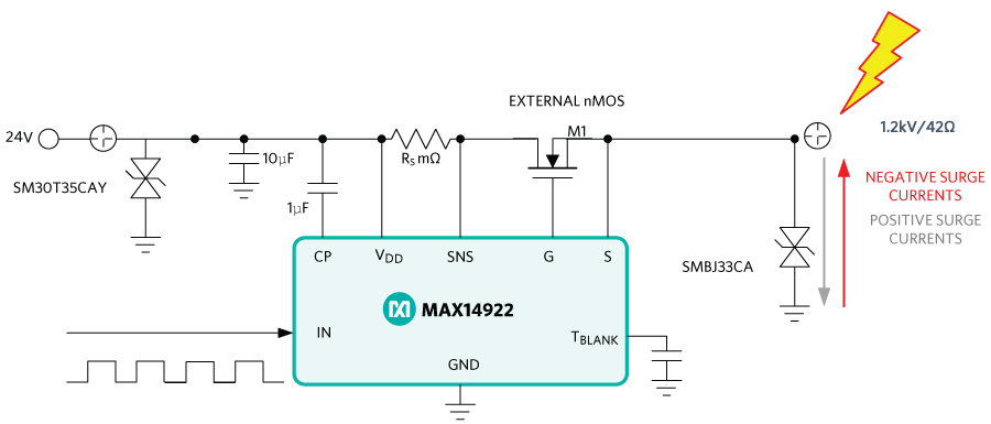
Figure 5a. Surge protection for 24V application.
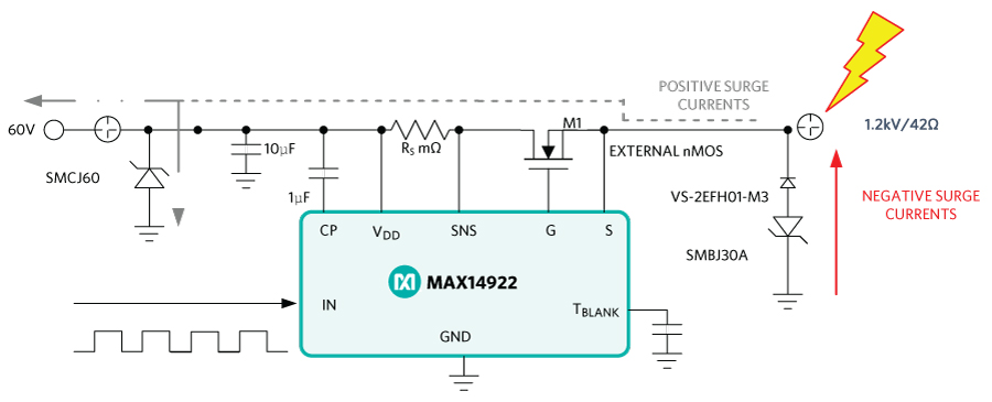
Figure 5b. Surge protection for 60V application.
Figure 5a shows the typical protection for a 24V application. The TVS diode at the S terminal of MAX14922 absorbs the surge energy through it. The level of surge capability of the application is dependent on the choice of the TVS characteristics (clamping current, power rating). The protection diode at the supply input (VDD) protects the supply side of the application.
Figure 5b shows the typical protection for a 60V application. A negative surge transient is dissipated by the TVS diode at the S terminal of MAX14922. The energy of a positive surge conducts through the body diode of the external FET and is absorbed by the TVS protection diode at the supply side (VDD).
Design Example
Let us look at how to design a high-side switch using the MAX14922 switch controller to meet these design targets:
- 60V max supply voltage (generally operating voltage is 24V or 48V)
- 2A nominal load current
- 1.2H maximum inductive load
- Withstands ±2kV surge (IEC 61000-4-5, 42O RSERIES)
- Operating temperature (-40°C to +85°C)
- Switching characteristics: duty cycle (~10%), frequency (0.5Hz)
- Minimum clamping voltage for inductive demagnetization of -33V
Determining the Sense Resistor RS
It is important to consider the tolerances and temperature coefficient for the series sense resistor RS and the current limit voltage threshold VCL. The variations caused by the tolerance and temperature coefficient add margin on the range of operating current as:

where ITRIP is the maximum current allowed in the application. When the load current exceeds the set current limit, the MAX14922 actively controls the MOSFET VGS to regulate the load current to ITRIP.
The VCL tolerance is ±10%, with a sense resistor RS with tolerance of 1% and a ±300ppm temperature coefficient. The trip current maximum and minimum limits are calculated as following with 2A as the working current:
Maximum current limit:

Minimum detected current limit:

The nominal rated load current level must be less than the ITRIP_MIN level to ensure proper function. The temperature coefficient of the sense resistor (TCR) contributes less than 1mO change from 25°C to 125°C temperature variation for sense resistor values of less than 20mO if it is kept under 300ppm.
Choose RS considering a 12mO with temperature change of -40°C to +85°C.
Considering a 12mO sense resistor, the following are the considerations of tolerance VCL and RSENSE put together for the given temperature range of -40°C to +85°C:

33mV/11.8m? RS (-1% - 300ppm TCR) (11.88m - 0.09m) = 2.8A
This value must be less than the maximum rated current of the load ITRIP_MAX.
RS = 12m? is an acceptable value for the given condition.
Determining the External N-Channel MOSFET
Based on a minimum inductive clamping voltage to achieve fast demagnetization of inductive loads, a TVS can be found with maximum clamping voltage of 40V.
- Total VDSS voltage at clamp is (VDD - VCLAMP_MAX) = 100V.
- The choice of the n-channel MOSFET must have VDSS greater than or equal to at least 100V. Allowing for variation in the VDD voltage, although the working voltage is 60V (maximum) and tolerances in clamping voltage, the maximum VDSS of the chosen FET must be = 100V.
- Choose a MOSFET with triode region RDSON.
- Keep in mind that MAX14922 can drive FETs with QG < 40nC. The following MOSFETs are a few options:
- Si7322DN (with 100V), 18A, 48mO RDSON with 13nC of gate charge.
- FDD770N15A, 200V, 18A, 77mO RDSON with 11nC of gate charge.
Choosing the TVS
Selecting the TVS considering surge/demagnetization parameters:
- Assuming a clamp voltage of 33V (unidirectional).
- All the energy is dissipated through the TVS diode during surge and inductive demagnetization. For ±2kV surge protection, the TVS must be able to handle peak surge currents of 48A.
Demagnetization
For VDD_MAX = 60V, VCLAMP = -36V, ILOAD = 2A, and L = 1.2H:
- The demagnetization time tDEMAG = 39.2ms obtained from Equation 3
- Peak power = 2A x (36V) = 2A x 36 = 72W and the energy stored in the inductor = 2.4J (from Eqn4 and Eqn1)
- ECLAMP = 0.5 x 36V x 2A x 39.2ms = ~1.413J. from Equation 5
- The 72 W is the peak power dissipated by the TVS (36V x 2A) or the average power for 39.2ms is 36W (PAVG_DEMAG). The equivalent DC resistor of the load dissipates part of the stored energy as heat through this equivalent resistance.
Frequency of Operation
The average power dissipated by the TVS due to inductive demagnetization during a continuous 2Hz switching is:

tPERIOD = tOFF + tON, (the time taken for repeated switching cycle).
Equation 9 determines the maximum switching rate of the application with the PAVG TVS within the steady state derated curves (Figure 6) of the TVS diodes. For a 0.5Hz switching and 10% duty cycle:
PAVG_TVS = (39.2ms/((2s) x PAVG_DEMAG = 0.72W
TVS diodes with the steady-state derating curve provide information on temperature, which is useful to determine the right type of TVS (in this case SMC33A from Bourns, Inc.). The average power must be within the derated curve of the TVS diode characteristics.
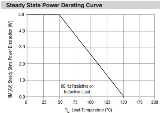
Figure 6: Steady-state power derating curve of the TVS Diode. Courtesy Bourns Inc. 1.5SMC data sheet.
The above curve provides a steady-state power dissipation of the clamp with respect to its lead temperature. The junction to lead thermal resistance and junction to ambient thermal resistance are available for the SMC package. It can be determined from the available information if the clamp used is within safe operating specifications for the entire ambient temperature range.
The junction temperature of the SMC package during steady-state dissipation is 139°C with the maximum ambient temperature at +85ºC. The lead temperature is 128°C with the junction temperature determined.
For a clamp, when subjected to demagnetization with a constant 0.5Hz switching cycle, it dissipates a steady-state power of 0.72W from the clamp and is within the derated curve of Figure 6 at maximum operated temperatures.
Clamp consideration with lower switching rates: When the load is seldom switched (once per hour or day), the peak power dissipation for a non-repetitive pulse vs. pulse duration aids in selecting the clamp. The steady-state derated curve is used when the switching is repetitive, more often it is a worse case design target as compared to the reduced/ lower rate of load switching (< 0.1Hz).
Including a Zener diode like the SMCJ60A at the VDD input supports the surge current requirements. Use a fast recovery epitaxial diode to avoid TVS clamp turn-on during the +60V normal operation. Figure 5b shows typical surge events and clamping action of the application. Figure 5b shows the current path in the event of a surge and the clamping action of the TVS diode.


