Low Power Op Amps: Only 20μA for 1.3MHz, 240μA for 30MHz
Our op amp family has expanded with industry-leading speed versus supply current. For super low 20μA supply current, the LTC6258/LTC6259/LTC6260 (single, dual, quad) provide 1.3MHz at a with 400μV maximum offset voltage and rail-to-rail input and output. The still-low 240μA of the LTC6261/LTC6262/LTC6263 (single, dual, quad) provide 30MHz with 400μV maximum offset voltage and rail-to-rail input and output. In combination with 1.8V to 5.25V supply, these op amps enable applications requiring good performance with low power and low voltage.
Low Noise Reference
One such application is a low noise reference based on the LT6656 precision series voltage reference with a low 1μA supply current. In combination with a simple filter, the LTC6258 can lower the LT6656’s effective noise and enhance its output current drive capability while maintaining low total power consumption.
Figure 1 shows the configuration. First, a very low cutoff frequency follows the LT6656 output (RIN1 and CIN1, lower than 5Hz cutoff). Large values of RIN1 can develop significant offset voltage due to the LTC6258’s input bias current. Setting RIN1 to 2.7kΩ produces an offset that is lower than the nominal input offset voltage of the op amp. CIN1 can be larger or smaller, with more or less filtering accordingly. The voltage withstanding requirement of CIN1 is low, resulting in relatively large capacitance in a small volume.

Figure 1. Low noise reference.
This circuit takes advantage of the ability of the LTC6258 to drive large capacitive loads. Use of a large output capacitor bank attached to the LTC6258 enables significant bypassing of follow-on circuits that use the reference voltage. In total, the combination of LT6656 and LTC6258, in this configuration, develops a reference voltage with low noise, at low power, and with appreciably large by pass capacitance.
Voltage spectral noise densities are shown in Figure 2. Greater noise from the reference below 10kHz drops down once a filter (RIN1 and CIN1) follows the reference. The op amp, configured in unity gain, with or without a large 44μF load, remains stable and contributes only a small amount of low frequency noise. Figure 3 shows the transient response of the combination of RIN1 – CIN1 filter and op amp circuit, with and without the 44μF output capacitor.
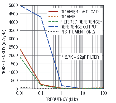
Figure 2. Buffer noise density.
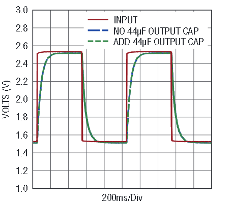
Figure 3. Reference buffer transient response.
Importantly, there is no appreciable degradation in the output voltage accuracy with the introduction of the LTC6258 into the reference circuit.The LT6656A-grade accuracy is 0.05%. At 1.25V, the error is ±625μV; the B-grade with 0.1% the error is ±1.25mV. Use of the LTC6258 with 400μV offset max will add some nominal output voltage uncertainty, but well within the order of magnitude of the LT6656’s initial error. Measured supply current consumption is 21μA.
Utility Sine Wave
One does not expect to generate a sine wave with –100dBc distortion using a 5V low power op amp. All the same, a bandpass filter using the LTC6258 can combine with an easy-to-use low power oscillator to create a sine wave at low cost, low voltage and extremely low dissipation.
Active Filter Component
The bandpass filter of Figure 4 is AC coupled to an input. As a result, the LTC6258 input does not place a burden on the previous stage to develop a particular absolute common mode voltage. A simple resistor divider with RA1 and RA2 provides biasing for the LTC6258 bandpass filter. Pegging the op amp inputs to a fixed voltage helps to reduce distortion that might arise with moving common mode.
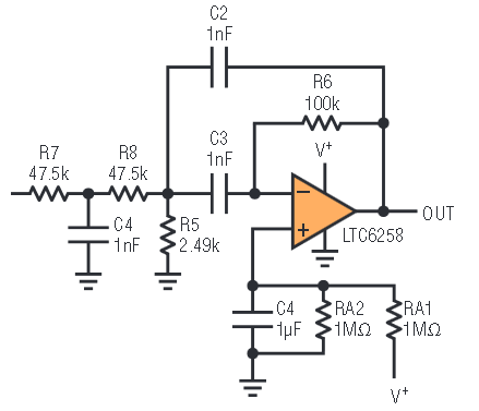
Figure 4. 10kHz bandpass filter.
This filter is centered at 10kHz. The exact resistance and capacitance values can be tweaked upward or downward, depending on whether lowest resistor noise or lowest total supply current is most important. This implementation is optimized for low dissipation by reducing current in the feedback loop. The capacitors C2 and C3 were initially 4.7nF or higher, with lower resistor values, but replaced with 1nF and higher resistor values, optimizing for lower dissipation.
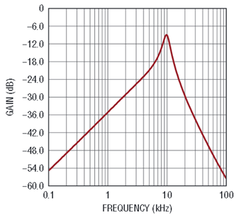
Figure 5. Bandpass filter gain/phase vs frequency.
Besides power dissipation, a secondary but no less important aspect of feedback impedance is loading of the op amp rail-to-rail output stage. Heavier loading, such as between 1K and 10K impedance, significantly lowers open loop gain, in turn affecting the accuracy of the bandpass filter. The data sheet suggests AVOL reduces by a factor of 5 from 100kΩ to 10kΩ. Lower C2 and C3 might be feasible, but then R6 becomes even larger, introducing more noise at the output.
The target Q of this bandpass filter is moderate, approximately 3. A moderate Q, rather than a high Q, allows use of 5% capacitors. Higher Q demands more accurate capacitors, and very likely higher open loop gain at 10kHz than is available with the feedback impedance load. Naturally, moderate Q results in less attenuation of harmonics than a higher Q.
Adding the Oscillator
A low power sine wave generator can be derived by driving a square wave into the bandpass filter. A complete schematic is shown in Figure 6. The LTC6906 micropower resistor set oscillator easily configures as a 10kHz square wave, and can drive the relatively benign loading seen in the bandpass filter input resistors. Supply current of the LTC6906 at 10kHz is 32.4μA.
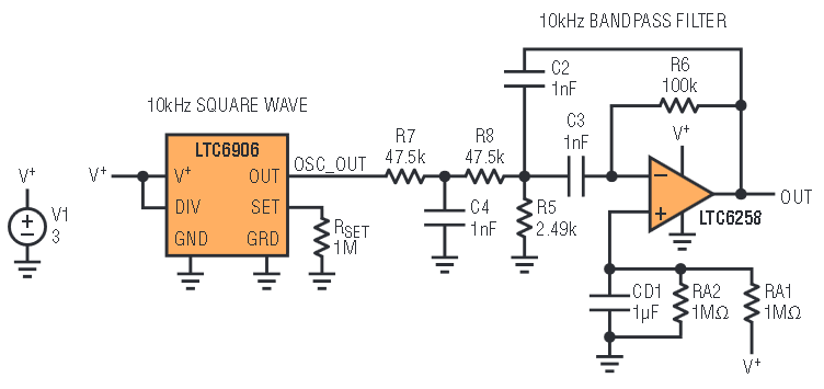
Figure 6. 10kHz oscillator circuit using LTC6906 TimerBlox® input.
Figure 7 shows the LTC6906 output and bandpass filter output. HD2 of the sine wave is −46.1dBc, and HD3 −32.6dBc. The output is 1.34VP-P to 1.44VP–P with the exact level varying slightly due to finite op amp open loop gain at 10kHz. Total current consumption is below 55μA on a 3V rail.
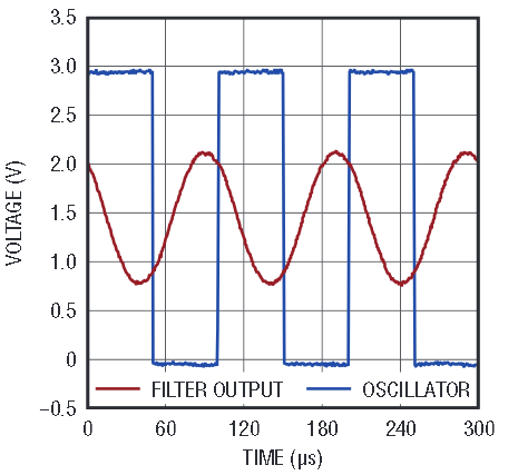
Figure 7. Voltage waveforms oscillator and filter output.
Other Enhancements
Figure 8 shows optional enhancements. A low power reference takes advantage of the ability of the LTC6906 and LTC6258 to operate on a very low supply. The reference provides 2.5V from a battery input. The fixed 2.5V supply stabilizes the output voltage swing in the presence of varying input voltage. In addition, even lower filter capacitor values with higher resistances reduce LTC6258 loading further, lowering dissipation and improving filter accuracy.
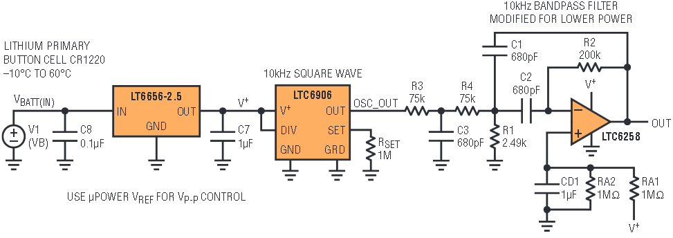
Figure 8. Oscillator and filter with a regulated supply.
Self-Oscillating LED Driver
LED blinking is an application where one would consider a microprocessor to provide simple control of a clock and duty cycle. Indeed, a microprocessor with a current limited output directly driving an LED offers the most direct implementation; the addition of a MOSFET with the LED and a current limiting resistor in the drain allows more current. These examples, however, do not provide means to control the LED current (LED brightness) without some additional circuitry. And, of course, a microprocessor adds the burden of code version control and maintenance, development platform, and programming steps in production.
Figure 9 shows an LED blinker with control of the ON LED current, without the use of a digitally synthesized frequency. R2 and R3 bring in a divided down copy of the supply voltage as a reference into the positive terminal. The op amp forces this voltage on the sense resistor RSENSE in LED ON operation.
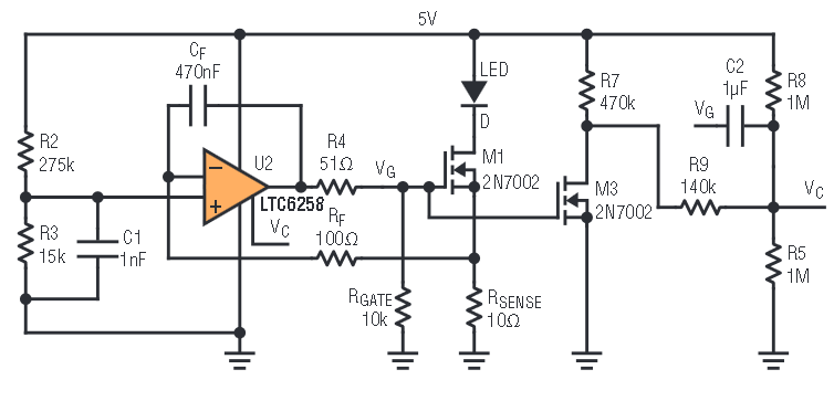
Figure 9. LED driver with self-oscillation.
The circuit of Figure 9 combines edge detection with use of the SHDN pin of the LTC6258. C2 can AC couple any fast VG gate drive action into the signal VC. Hence, when the gate voltage of M1 increases when LED ON begins, VC suddenly rises. VC connects to the SHDN pin; a rising edge on the SHDN pin enables the LTC6258, which is already driving LED current through its feedback circuit, to stay on. However, M3 is also on while M1 is on, and as a result works with R9 to charge C2 slowly until VC falls below the SHDN threshold. At that moment, the active low shutdown kicks in, and the LTC6258 turns off. A negative falling VG voltage again feeds through C2, and a falling VC and hence a falling SHDN pin voltage keeps the circuit in an “LED OFF” state for some time. M3 turns off, and C2 discharges until VC is high enough to reactivate the LTC6258.
It may seem a bit odd to develop such a circuit when a microprocessor or a LTC6992 can provide on-off capability in combination with a single MOSFET and resistor. The problem with those circuits, however, is the lack of control over the LED current. In the circuit of Figure 9, a voltage is controlled across a sense resistor. The LED voltage is independent of LED drive current. The generation of the on-off, or blinking, comes with the addition of a handful of low cost components.
It is interesting to note that the LED current depends on the supply in this implementation inasmuch as the supply feeds the reference through R2 and R3. The supply figures into the time of the on and off cycle since the supply powers the edge detection and relaxation part of the circuitry. When the supply falls, the LED current drops and the cycle time increases. This change of behavior can help in battery powered LED blinking applications to predict end of life. Alternatively, with a reference such as the LT6656 powering the entire circuit except for the LED and M1 branch, operation with unchanging LED brightness and frequency is possible.
Figure 10 shows the sense resistor voltage and the SHDN pin voltage. The SHDN voltage is tied to VC; the gate drive couples through C2 as previously described.
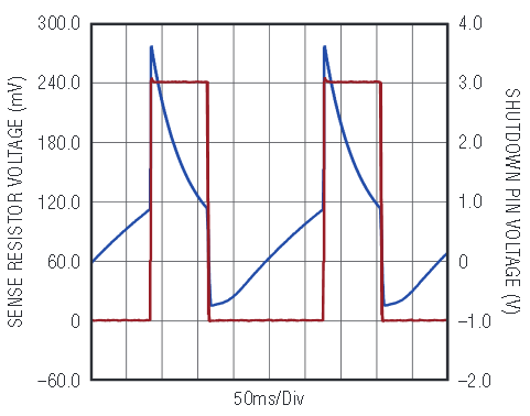
Figure 10. LED blinker current.
Components RF and CF can significantly slow edges down. Adding this much delay is not essential, but it can help to smooth out any hiccups that occur when the part goes through a power up sequence after the SHDN pin goes inactive high. The 47μs time constant (RF•CF) is insignificant in the time scale of the blinking (tens or hundreds of ms)—47μs is much smaller than any time constant associated with C2 and its resistors.
Active Filters
The LTC6261/62/63 op amps’ high MHz-to-mA ratios can freshen up traditional filter circuits. The two filter examples discussed here display performance previously unachievable with such low power.
Second Order Bessel Filter
Ample bandwidth and low supply current enable deployment of active filters in portable and other low power applications. For instance, a second order Bessel filter, shown in Figure 11, provides a clean transient response at the expense of a less steep roll-off in the frequency domain.
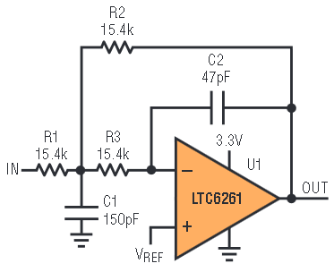
Figure 11. Second order Bessel filter.
Measured supply current consumption is about 230μA, although data sheet supply maximum values suggest that the consumption across production and temperature may be slightly higher. The values of resistors chosen minimize consumption at the expense of in-band noise.
If VREF is derived from a high impedance resistor divider, then a large capacitor is required to ensure that the reference voltage is solid down to very low frequencies. The reference at the positive op amp input must be a good “AC ground” at all frequencies when using this inverting amplifier configuration.
| GBW | IS perAMP | GBW EFFICIENCY, MHz/mA | SR EFFICIENCY, Vμs/mA | enEFFICIENCY, (nV√Hz)•√mA | |
| LTC6258/9/60 | 1.3MHz | 20μA | 65 | 12 | 38 |
| LTC6255/6/7 | 6.5MHz | 65μA | 100 | 24 | 5.5 |
| LTC6261/2/3 | 30MHz | 240μA | 125 | 29 | 13 |
| LTC6246/7/8 | 180MHz | 1mA | 180 | 90 | 4.2 |
| LTC6252/3/4 | 720MHz | 3.5mA | 206 | 80 | 5.1 |
The frequency response (Figure 12) shows an expected roll-off of two poles along with a gentle droop near the 3dB point; the transient response is very clean, as shown in Figure 13.
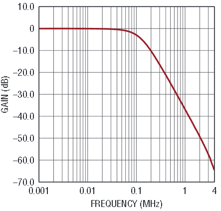
Figure 12. Second order Bessel frequency response.
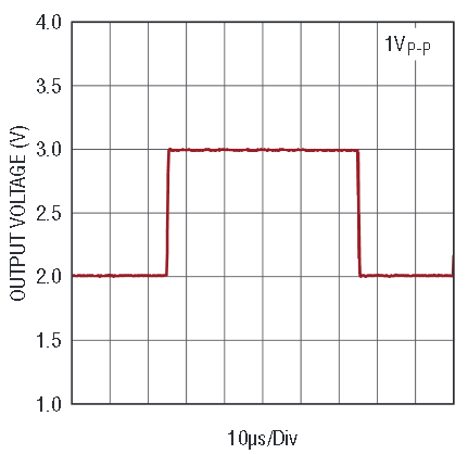
Figure 13. Bessel filter transient response.
Third Order Butterworth Filter
Maximally flat magnitude response in the passband arises from use of a Butterworth filter. An extra RC stage is added in front of the filter in order to maximize the roll-off for a single amplifier circuit. Use of an extra stage complicates the math, but not intractably so.
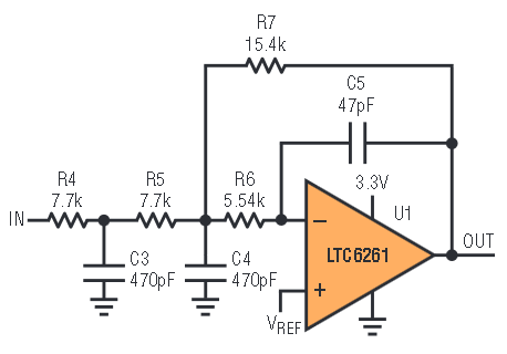
Figure 14. Third order Butterworth filter.
Measured supply current consumption is about 235μA. The chosen values of resistors minimize consumption at the expense of in-band noise.
The frequency response (Figure 15) shows an expected roll-off of three poles, an extended plateau and a sharp roll-off; the transient response includes a small amount of ringing as shown in Figure 16.
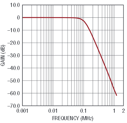
Figure 15. Third order Butterworth frequency response.
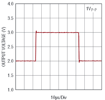
Figure 16. Butterworth filter transient response.
Bridge-Tied Differential Output Amplifier
The low supply current of these op amps at the bandwidth and noise performance allows for excellent fidelity at a fraction of the usual dissipation in portable audio equipment. As with active filters, revisiting portable audio equipment headphone drivers is a rational enterprise, given the unique capabilities of the LTC6261.
One significant concern in a portable device is battery drain. Music played loudly, or listeners’ musical choices affect the rate of battery drain for the most part, the end-use of a device is out of the designer’s control. Quiescent current, though, is not. Because much of a device’s time may be spent idle, quiescent current is significant, as it drains batteries continuously. The LTC6261’s low quiescent current increases battery discharge time.
Headphone speaker impedances range from 32Ω to 300Ω; their responsivity, from 80dB to 100dBSPL per 1mW and beyond. As an example, considering a headphone speaker with 90dBSPL per 1mW, it takes 100mW delivered to reach 110dBSPL.With 32Ω, the RMS current is 56mA and voltage 1.8V; with 120Ω,29mA and 3.5V.
Given a 3.3V supply and the output of one LTC6261 amplifier, there may not be sufficient drive capability to yield 100mW. However, the combination of two 180° phased amplifiers is enough to provide the necessary drive to reach upwards of 100mW delivered power. Duplication of this bridge drive circuit enables power to both left and right sides. Figure 17 shows the driver schematic.
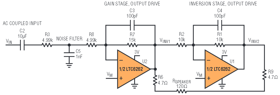
Figure 17. Audio headphones bridge driver.
The LTC6263 provides four amplifiers in one small package. Data from a 2-amplifier LTC6262 driving what could be left or right is shown in Figures 18 and 19. Basic current consumption of the two amplifiers, with as much as 1VP-P input but no load, is 500μA.
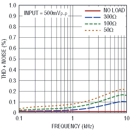
Figure 18. LTC6262 bridge driver THD and noise with different loads vs frequency.
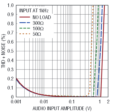
Figure 19. LTC6262 bridge driver THD and noise with different loads vs amplitude at 1kHz.
The solution shown in Figure 17 consists of first, an inverting gain stage with closed loop gain = 1.5, and a subsequent inverting stage. The combination of inverting stages produces a single-ended input to differential output gain of 3. With 500mVP-P input, the output is 1.5VP-P, or 0.75V max, or 0.53VRMS. With 50Ω, 500mV input leads to approximately 5.6mW delivered power. At 1VP-P input, the circuit delivers 22.5mW. Note that it helps that the LTC6261 output can swing close to rail-to-rail with load.
The first build of this circuit in the lab produced a significant tone at a few hundred Hz. It turned out that the positive input was not well grounded as an “AC ground” over all frequencies because the voltage was not strongly pegged. The need to peg the voltage arises when using a single supply rather than a dual supply. With a single supply, VM is not ground, but rather a mid-rail voltage created to enable inverting topologies to work properly. The resistor divider that creates VM has large resistance values (for example, two 470k in series) to minimize additional supply current. A large capacitor ensures a strong ground at low frequencies. Indeed, the addition of a large capacitor (1μF, which forms a pole with the 470k resistors in parallel) eliminates the mysterious distortion tone.
Despite the low quiescent current, this driver delivers low distortion to a headphone load. At high enough amplitude, distortion increases dramatically as the op amp output clips. Clipping occurs sooner with more loading as the output transistors start to run out of current gain.
Conclusion
The applications shown here take advantage of a unique combination of features available in the LTC6258/LTC6259/LTC6260 and LTC6261/62/63 op amp families. The low quiescent current of these devices does not diminish their ability to perform at levels usually reserved for more power hungry parts. Rail-to-rail input and output, shutdown, and choice of package are features that add to their versatility.


