Low Power, DC Accurate Drivers for 18-Bit ADCs
A common misconception about 18-bit SAR ADCs is the only way to drive them is with a high powered, high speed, low noise op amp or differential driver whose DC performance often leaves much to be desired. It is possible to use a low power, DC accurate op amp to drive an 18-bit SAR ADC if the input is a DC or low bandwidth AC signal and the op amp outputs are given sufficient time to settle. Using the single-ended to differential driver of Figure 1, four different low power dual op amps were tested to show the trade-offs in using low power drivers.
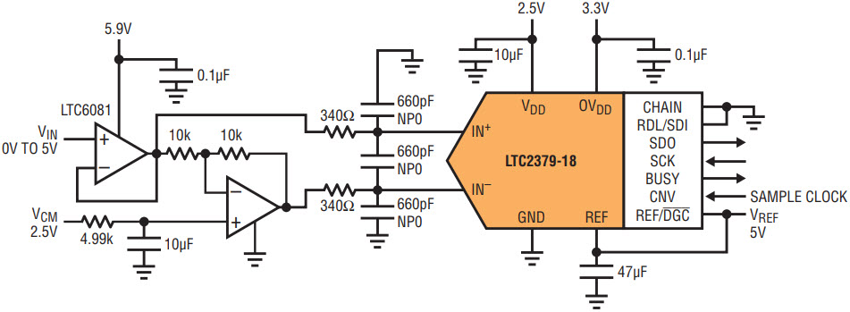
Figure 1. Low power, DC accurate single-ended to differential driver for the LTC2379-18.
This circuit enables the testing of offset voltage, the maximum sample rate for DC and AC signals, noise and power consumption. The ADC used is the LTC2379-18, a 1.6Msps 18-bit SAR ADC with an offset of ±9LSBs, INL of ±2LSBs and peak-to-peak noise of 5LSBs.
The four amplifiers used are the LT1013, LTC6078, LTC6081 precision and LTC2051HV zero-drift dual op amps—Table 1 shows a summary of their major specs. The circuit supply voltage is the voltage applied to the V+ and V– terminals of the op amps. This voltage determines the power dissipation of the amplifier and its maximum signal swing. The voltages were chosen to maximize undistorted signal swing without exceeding the maximum ratings of the amplifiers or unnecessarily increasing power dissipation.
| Part | ISY (µA) Typ/Amp | VOS (µV) Max | Circuit Supply Voltage (V) |
| LT1013A | 350 | ±150 | 8, –3 |
| LTC2051HV | 1000 | ±3 | 8, –3 |
| LTC6078 | 55 | ±30 | 5.9, 0 |
| LTC6081 | 340 | ±70 | 5.9, 0 |
Offset Volatage
The worst-case offset of the LTC2379-18 is only ±340µV. As Table 1 shows, the offset voltage of these four op amps is even lower, varying from ±3µV max for the LTC2051HV to ±150µV max for the LT1013. To maintain this low level of offset voltage careful circuit design and layout practices are required. Examples of this include using the 4.99kΩ resistor in the positive input of the inverting amplifier to balance the input bias current created voltage drops and using symmetrical layout around the positive and negative inputs of the ADC, minimizing the effects of the parasitic elements.
Maximum Sampling Rate for DC Signals
Even with a DC input voltage there is some settling time required. When the ADC goes from hold mode to sample mode, the sample capacitor is switched onto the analog input pin of the ADC producing a brief transient. The sample capacitor is then charged by the op amp back to its final value.
The maximum sampling frequency for a DC input voltage can be determined by reducing the sampling frequency until there is no ripple on the sampled waveform. Take this measurement with the analog input near positive or negative full scale as this typically causes the largest transients to be generated at the analog inputs, which in turn require the maximum settling time. Maximum sampling rates for the four op amps vary from 63ksps to 230ksps. The maximum sample rates for the four op amps are shown in Table 2.
| Part | DC Input Maximum Sample Rate (ksps) |
| LT1013A | 185 |
| LTC2051HV | 230 |
| LTC6078 | 63 |
| LTC6081 | 165 |
Maximum Sampling Rate for AC Signals
For applications with a slow moving analog signal or a multiplexer at the driver input, determining the maximum sampling rate is more complex. With the potential for a full-scale swing from one measurement to the next it is necessary to consider the settling of the RC filter at the output of the driver circuit and the settling time of the op amp itself to an 18-bit level. Because settling to the 18-bit level is almost never specified, it must be experimentally determined.
Drive the op amps with a flat falling edge as shown in Figure 4 so that the settling of the op amps is measured; not the slow change of the DC input. The schematic for the edge shaping circuit is shown in Figure 2.
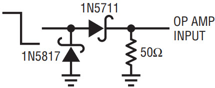
Figure 2. Schottky diodes flatten falling edge of input pulse.
It is important to keep the stray capacitance on the op amp input as small as possible to minimize the settling time of this circuit. By swapping the outputs of the SE-Diff driver circuit of Figure 1 it is possible to look at both falling and rising edge settling times.
With the flat input edge in place, one can look at the ADC output to see how long the output of the SE-Diff driver takes to settle. One method involves using the PScope data acquisition software and carefully choosing the sample rate and input frequency. Using a 50kHz sample rate to ensure that all four op amps settle completely once the input signal is constant would normally only allow a 20µs resolution in the settling time measurement. By using the primitive wave capability of PScope and picking the sampling frequency, input frequency and sample size such that multiple passes of the input signal are sampled at different time slices it is possible to reassemble the samples to create a high resolution image of the input signal.
The formula used to determine the ratio of input frequency to sample frequency is

where N is the sample size. N must be 2i where i is any integer from 10 to 17 for PScope. M is any odd number from 1 to N/2. fS is the sample frequency and fIN is the input frequency. Picking a sample size of 131072 to maximize resolution, an input frequency of 250Hz and M = 653 to get a sample rate of approximately 50ksps yields an fS of 50.18070444ksps.
The full resolution shown is necessary, as the primitive wave requires an exactly coherent relationship between sample rate and input frequency. The clock and the input signal generator must be synchronized. Figure 3 shows the test setup. The strobe signal makes sure that PScope starts capturing at the same point for each series of samples and requires that Start on Trigger is enabled in the Tools menu. To calculate the required clock frequency, multiply the desired sample frequency by 62 when using the DC1783A-E. This results in an input clock frequency of 3.111203675MHz.
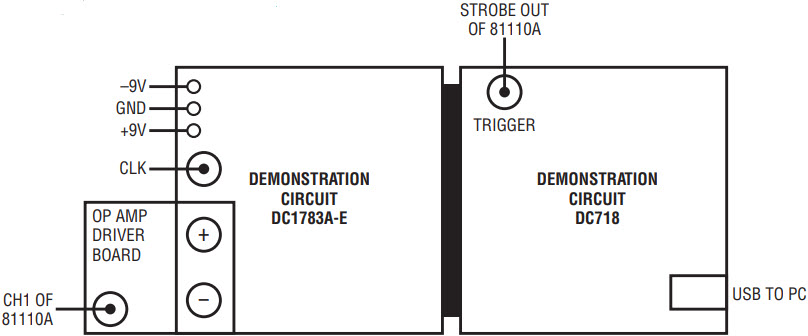
Figure 3. Data acquisition setup.
The PScope output for the LT1013 is shown in Figure 4. With 131072 samples divided into the 4ms period of the input waveform, a resolution of 30.5ns/point is achieved. By zooming in on the start and stop points of the primitive waveform it is possible to calculate an approximate settling time. This is limited by the peak-to-peak noise. To increase the accuracy of this measurement, it is possible to take the raw data from PScope, export it to Excel or MATLAB, and then reassemble the primitive wave and average the resulting data. The raw results as well as the averages of 16 readings and 64 readings for the four op amps are shown in Figures 5–8. The settling times and peak-to-peak noise are summarized in Table 3. Note that the LTC2051HV, which had the fastest sample rate for a DC signal has the slowest settling time for a full scale input swing. This is a result of the time required to auto-zero the difference in offset voltage caused by the change in common mode input voltage.
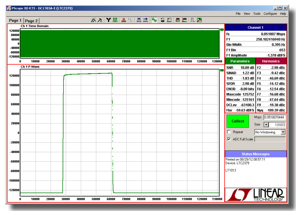
Figure 4. PScope primitive wave shows LT1013 settling time for falling edge with 30.5ns/sample resolution.
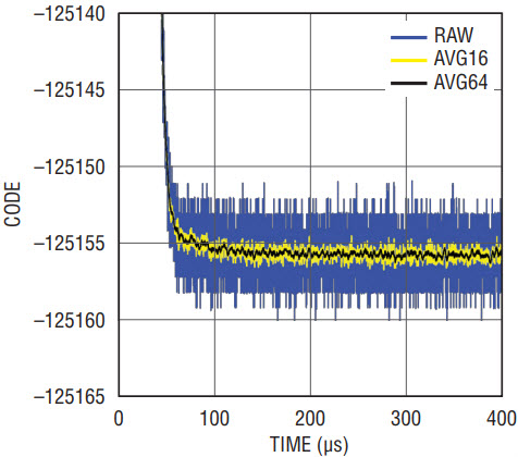
Figure 5. LT1013 settling.
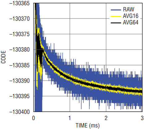
Figure 6. LTC2051HV settling.
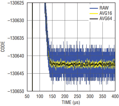
Figure 7. LTC6078 settling.
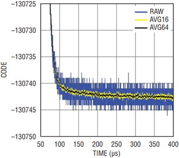
Figure 8. LTC6081 settling.
| Part | Settling Time (µs) | PK-PK Noise (LSBs) | Average of 16 Samples PK-PK Noise (LSBs) | Average of 64 Samples PK-PK Noise (LSBs) |
| LT1013 | 80 | 10 | 2.2 | 1.1 |
| LTC2051HV | 3000 | 14 | 2.9 | 1.2 |
| LTC6078 | 140 | 12 | 3.3 | 1.7 |
| LTC6081 | 130 | 8 | 1.8 | 0.9 |
Removing the Schottky diodes and driving a 20Hz sine wave into VIN of the SE-Diff input with a sampling frequency of approximately 1/(settling time) yields the THD numbers for the circuit of Figure 1 shown in Table 4. Good THD numbers are an indication of the linearity of the circuit.
| Part | fS (kHz) | THD (dB), AIN = –1dBFS |
| LT1013 | 12.0 | –105 |
| LTC2051HV | 0.3 | –104 |
| LTC6078 | 7.0 | –98 |
| LTC6081 | 7.0 | –105 |
Noise
As shown in the summary of Table 3, the combination of the SE-Diff driver and the LTC2379-18 yields a peak-to-peak noise that is 1.5 to 3 times higher than the ADC by itself. With relatively modest averaging it is possible to obtain noise levels that approach 1LSB peak-to-peak. As long as the noise is Gaussian and not caused by clock feedthrough or some other synchronous source, averaging should reduce the noise by the square root of the number of the samples. Averaging reduces the effective sampling rate and may not be practical with non-repetitive AC signals.
Power Consumption
Table 5 shows the power dissipation of the op amps and the LTC2379-18 at the maximum DC and AC sampling frequencies of the single-ended to differential data acquisition circuit of Figure 1. The op amp power dissipation is per amplifier and does not change with sampling frequency because the op amps are always on. The LTC2379-18 power dissipation is linear with sampling frequency due to its auto shutdown after a conversion. The combined circuit power dissipation in columns four and six of Table 5 shows the dissipation of the two op amps and the LTC2379-18 used in the circuit added together. At the higher sampling rates that are possible with DC input signals, the power dissipation of the LTC2379-18 is a significant portion of the total. At the lower sampling rates required for AC or muxed input signals, the op amps dissipate almost all of the power for this circuit.
| Part | >Op Amp PD (mW) at Circuit Supply Voltage | LTC2379-18 PD (mW) at Max DC fS | Combined Circuit PD (mW) at Max DC fS | LTC2379-18 PD (mW) at Max AC fS | Combined Circuit PD (mW) at Max AC fS |
| LT1013 | 3.85 | 2.08 | 9.78 | 0.135 | 7.835 |
| LTC2051HV | 11.00 | 2.59 | 24.59 | 0.003 | 22.003 |
| LTC6078 | 0.32 | 0.71 | 1.35 | 0.080 | 0.720 |
| LTC6081 | 2.01 | 1.86 | 5.88 | 0.080 | 4.100 |
Conclusion
Using low power, DC-accurate op amps to drive 18-bit SAR ADCs is possible as long as enough time is allowed for the op amps to settle. Settling time is the limiting factor in determining the circuit’s maximum sampling rate, and varies greatly by op amp choice and the type of signal source, DC or AC. ADC offset and linearity can be maintained using low power op amps. Due to the higher noise of the low power op amps, some averaging may be required to reduce the noise at the expense of a lower effective sampling rate. At lower sample rates power dissipation is limited by the op amp driver circuitry, which must remain on so that it can settle, while the ADC can typically be powered down after only a brief conversion period. It is important to pick an op amp that is a good match to the offset, sampling rate, noise, linearity and power requirements of your overall circuit requirements.
关于作者
T他的职业生涯始于LTC,当时的职位是技术员,并向参与多个产品工作的Bob Dobkin、Bob Widlar、Carl Nelson和Tom Redfern学习,涉及产品包括运算放大器、比较器、开关稳压器和ADC。在此期间,他还花了大量时间来编写测试程序以对这些器件的特性进行表征。


