Low Noise Power Supplies Come in Many Flavors: Part 2 - Charge Pump Solutions
Low Noise Power Supplies Come in Many Flavors: Part 2 - Charge Pump Solutions
2017-03-23
Read other articles in this series.
Charge pump solutions are often thought to be too noisy for low noise applications. Engineers associate charge pump power supplies with peak-to-peak noise levels in the 20mV to 200mV range. Analog Devices' latest family of regulated charge pump plus linear regulator power supply solutions are inductorless, small size, low output noise devices that exhibit much lower noise than expected for a charge pump. These products are viable power supply alternatives for low noise systems.
The LTC3260 low noise charge pump plus linear regulator solution is shown below in figure 1. In this circuit, a 15V input voltage is converted to ±12V at 50mA. The 15V input is linear regulated down to 12V at output pin LDO+ and also inverted to give –15V; then the –15V output is linear regulated down to –12V at output pin LDO–.
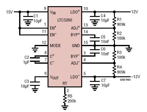
Figure 1. Low Noise Bipolar Supply Charge Pump Plus LDO Solution
The corresponding output noise on the inverting charge pump output (VOUT pin) is approximately 7mV peak-to-peak as shown in the digital scope plot below, while the noise on the LDO outputs (pins LDO+ and LDO–), is indistinguishable from the trace itself when viewed on a 10mV per division y axis scale.
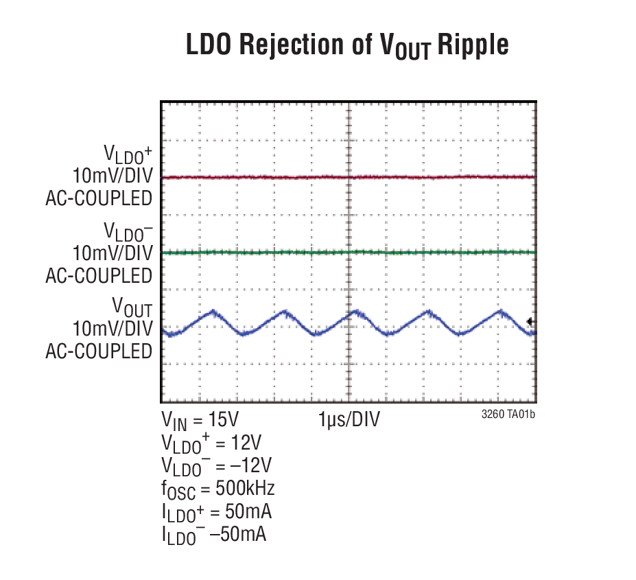
Figure 2. Output Noise with 15V input to ±12V Outputs
To see the noise in more detail, a precision, a high performance analog scope is used. To isolate the linear regulator noise, the circuit is observed without the charge pump switching. Figures 3a and 3b show the linear regulator output noise, with the charge pump disabled.
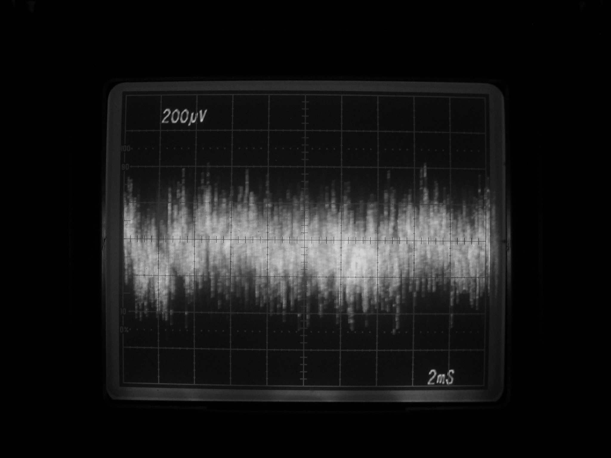
Figure 3a. LTC3260 Positive LDO Output Noise
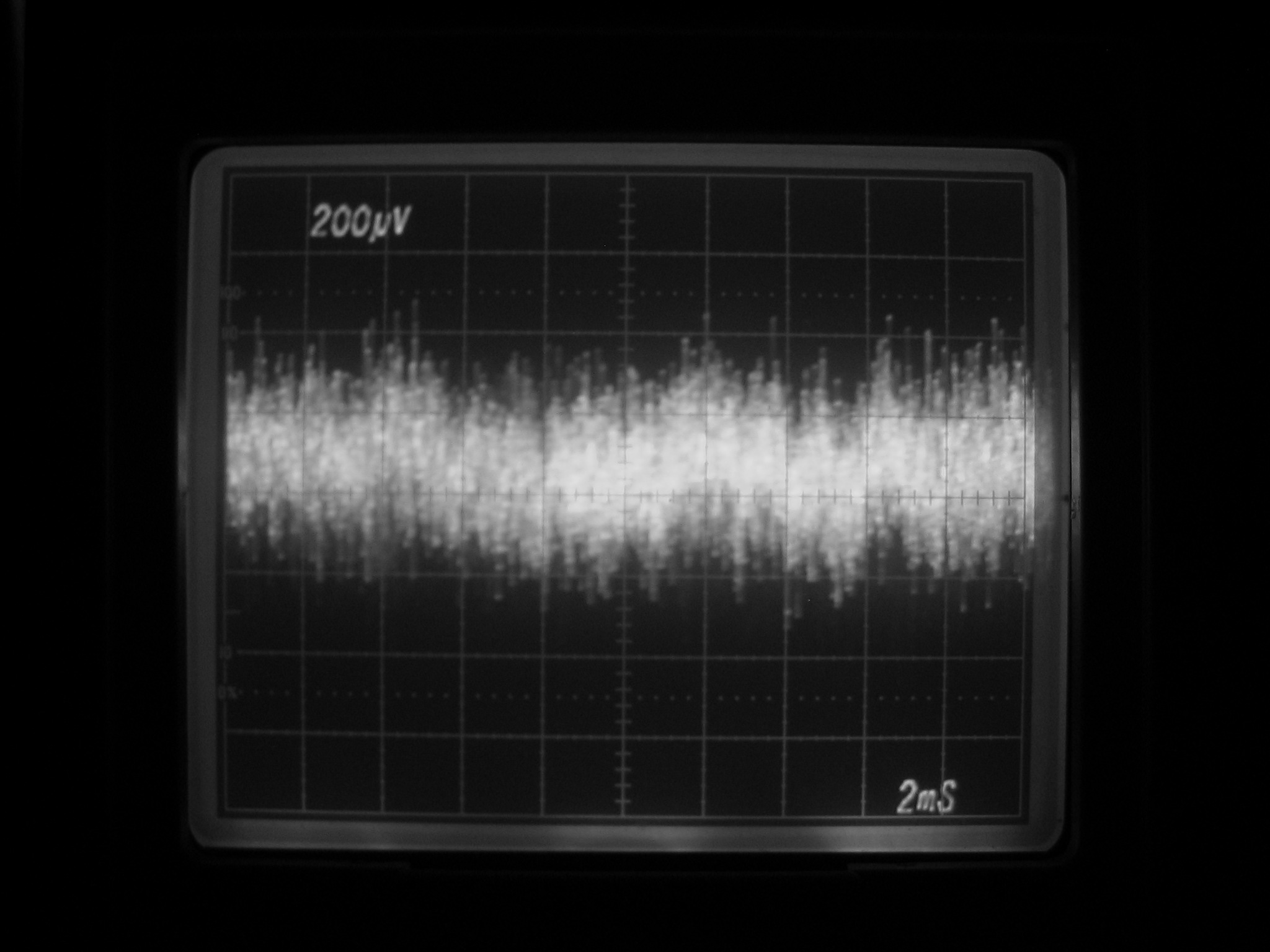
Figure 3b. LTC3260 Negative LDO Output Noise
6.5V was applied at the VIN input and –6.5V was applied at VOUT and the circuit was configured to provide a ±5V output at 50mA. In both cases, the peak-to-peak noise is less than 800µV. Since the noise is not truly Guassian, we cannot simply divide by six to the equivalent RMS output noise, but instead must use a larger value. The effective RMS noise due to the linear regulator is around 100µV. This low noise linear regulator rejects most of the attenuates charge pump switching noise.
With low output currents (i.e. less than approximately 8mA), the LTC3260's efficiency and noise performance can be traded-off using the MODE pin. Burst Mode operation offers highest efficiency and lowest quiescent current (100µA), but increases output noise, while forced continuous operation provides the lowest noise at the expense of efficiency (3.5mA quiescent current). With heavy loads the device operates with continuous switching, minimizing subharmonic ripple noise. Keep in mind that with all linear regulators, thermal performance must be taken into consideration to prevent excessive heat dissipation.
Analog Devices' charge pump plus linear regulator solutions provide low noise performance and can be used in designs sensitive to noise. Their wide input voltage range extends their use well beyond 5V applications. The LTC3265 is similar to the LTC3260 but adds a 2× boost charge pump on the input voltage in addition to the inverting charge pump and LDOs. A table of our charge pump plus LDO solutions is given below.
| LTC3260 | LTC3265 | |
| Function | Inverting charge pump plus positive and negative 50mA LDOs | Boost (2× VIN) and inverting charge pumps plus positive and negative 50mA LDOs |
| Example solution | 15V to ±12V @ 20mA | 12V to ±15V @ 20mA |
| Input Voltage (V) | 4.5 to 32 | 4.5 to 16 |
| Burst Mode Operation or Low Noise Constant Frequency Switching | pin-select | pin-select |
Devices like the LTC3260 and the LTC3265 dispel the notion that charge pump solutions are too noisy for low noise systems. These devices may be the perfect fit when an inductor-based solution is not desired or when good noise performance is needed but the ultimate in noise performance is not required and the noise performance requirements are more stringent than those offered by conventional charge pump solutions.
In Part 3 of this series, we look at low noise switching regulators.
