摘要
Timing jitter, edge speeds, aberrations, optical dispersion, and attenuation all impact the performanceof high-speed clock recovery for SDH/SONET receivers. These effects decrease the time available for error-free data recovery by reducing the received \"eye opening\" of nonreturn-to-zero (NRZ) transmitted signals. Optical receivers, incorporating transimpedance preamplifiers and limiting postamplifiers, can significantly clean up the effects of dispersion and attenuation. In addition, these amplifiers can provide fast transitions with minimal aberrations to the subsequent clock/data recovery (CDR) blocks. However, these stages also add distortions to the midpoint crossing, contributing to timing jitter. Timing jitter is one of the most critical technical issues to consider when developing optical receivers and CDR circuits.
1 Introduction
Timing jitter, edge speeds, aberrations, optical dispersion, and attenuation all impact the performance of high-speed clock recovery for SDH/SONET receivers (Figure 1). These effects decrease the time available for error-free data recovery by reducing the received "eye opening" of nonreturn-to-zero (NRZ) transmitted signals.
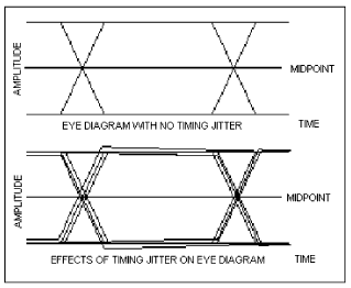
Figure 1. Eye diagram with and without timing jitter
Optical receivers, incorporating transimpedance preamplifiers and limiting postamplifiers, can significantly clean up the effects of dispersion and attenuation. In addition, these amplifiers can provide fast transitions with minimal aberrations to the subsequent clock/data recovery (CDR) blocks. However, these stages also add distortions to the midpoint crossing, contributing to timing jitter. Timing jitter is one of the most critical technical issues to consider when developing optical receivers and CDR circuits.
A better understanding of the different sources of jitter helps in the design and application of optical receiver modules and integrated CDR solutions. SDH/SONET specifications are well defined regarding the amount of jitter tolerance allowed at the inputs of optical receivers, as well as jitter-peaking requirements, but they do little to define the different sources of jitter. The jitter that must be tolerated at an optical receiver input involves three significant sources, all of which are present to varying degrees in typical receiver systems:
1) Random jitter (RJ)
2) Pattern-dependent jitter (PDJ)
3) Pulse-width distortion (PWD)
2 Random Jitter (RJ)
RJ is caused by random noise present during edge transitions (Figure 2). This random noise results in random midpoint crossings. All electrical systems generate some random noise; however, the faster the speed of the transitions, the lower the effect of noise on random jitter. The following equation is a simple worst-case estimation of random jitter:

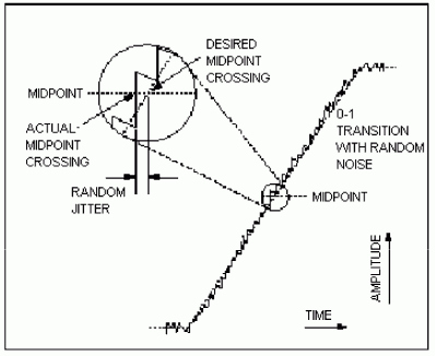
Figure 2. Random jitter on edge transition
3 Pattern-Dependent Jitter (PDJ)
PDJ results from wide variations in the number of consecutive bits contained in NRZ data streams
working against the bandwidth requirements of the receiver (Figure 3). The location of the lower -3dB cutoff frequency is important and must be set to pass the low frequencies associated with long, consecutive bit streams. AC-coupling is common in optical receiver design.
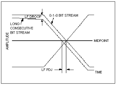
Figure 3. Pattern-dependent jitter due to low-frequency cutoff
When using a limiting preamplifier with a highpass frequency response, select the input AC-coupling capacitor into the postamplifier, CAC, in order to provide a low-frequency cutoff (fC) one decade lower than the preamplifier low-frequency cutoff. As a result, the PDJ is dominated by the low-frequency cutoff of the preamplifier.
When using a preamplifier without a highpass response, the following equation provides a good starting point for choosing CAC into the postamplifier:

where tL = duration of the longest run of consecutive bits of the same value (seconds); Rin = input resistance of the postamplifier; PDJ = maximum allowable pattern-dependent jitter, peak-to-peak (seconds); and BW = typical system bandwidth, normally 0.6 to 1.0 times the data rate (hertz). If the PDJ is still larger than desired, continue increasing the value of CAC. Note that to maintain stability, it is important to keep the low-frequency cutoff well below the corner frequency associated with the postamplifier.
PDJ can also be present due to insufficient high-frequency bandwidth (Figure 4). If the amplifiers are not fast enough to allow for complete transitions during single-bit patterns, or if the amplifier does not allow adequate settling time, high-frequency PDJ can result.
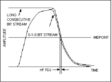
Figure 4. Pattern-dependent jitter due to high-frequency rolloff
4 Pulse-Width Distortion (PWD)
Finally, PWD occurs when the midpoint crossing of a 0-1 transition and a 1-0 transition do not occur at the same level (Figure 5). DC offsets and nonsymmetrical rising and falling edge speeds both
contribute to PWD. For a 1-0 bit stream, calculate PWD as follows:

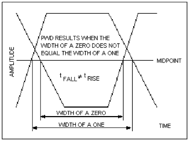
Figure 5. Pulse-width distortion
关联至此文章
产品
低功耗、622Mbps限幅放大器,带有无抖动功率检测输出,用于LAN
低噪声、光纤通道互阻放大器
2.7Gbps后置放大器,带有自动增益控制
四路SPST、超低泄漏、CMOS模拟开关
2.5Gbps、+3V至+5.5V、宽动态范围互阻前置放大器
1.25Gbps/2.5Gbps、+3V至+5.5V、低噪声互阻前置放大器,用于LAN
+3.0V至+5.5V、1.25Gbps/2.5Gbps限幅放大器
622Mbps、超低功耗,3.3V互阻前置放大器,用于SDH/SONET
+3.0V至+5.5V、1.25Gbps/2.5Gbps限幅放大器
+3.0V至+5.5V、1.25Gbps/2.5Gbps限幅放大器
+3.3V、2.5Gbps低功耗互阻放大器
不推荐用于新的设计
低功耗、622Mbps限幅放大器,带有无抖动功率检测输出,用于LAN
低噪声、光纤通道互阻放大器
+3.0V至+5.5V、1.25Gbps/2.5Gbps限幅放大器
1Gbps、高速限幅放大器,带有无抖动的信号消失检测
622Mbps、低噪声互阻前置放大器,用于LAN及WAN光接收器
622Mbps、超低功耗、3.3V互阻前置放大器,用于SDH/SONET
双速率、光纤通道限幅放大器
+3.0V至+5.5V、1.25Gbps/2.5Gbps限幅放大器

