Getting the Most Out of the MAX14920/MAX14921 High-Accuracy Battery-Measurement AFEs
摘要
The MAX14920/MAX14921 is a high-accuracy battery-measurement analog front-end (AFE) ideal for cell balancing and battery-measurement applications. The performance of the system in which the MAX14920/MAX14921 is used, however, depends highly on the components that support and surround it. This application note provides a framework for, and examples of, selecting system architectures and building blocks that meet diverse accuracy and cost requirements.
A similar version of this article appears on EDN, November 19, 2013.
Introduction
The MAX14920/MAX14921 are high-accuracy battery-measurement analog front-ends (AFEs) for monitoring up to 12 and 16 battery cell voltages, respectively. The excellent accuracy and unique sample-and-hold architecture of the MAX14920/MAX14921 is ideal for monitoring cell chemistries with nearly flat discharge curves, such as lithium phosphate cells, but it can also be used in applications where accuracy is not the tightest constraint.
As a building block, the overall performance of the MAX14920/MAX14921 is highly dependent on the network of ICs surrounding it. This application note provides a framework for, and examples of, selecting system building blocks that meet diverse accuracy and cost requirements.
Building a System that Meets Your Needs
While designing systems, engineers often face cost, space, and accuracy constraints that dictate how an engineering solution is constructed. Some systems, such as lithium phosphate cell monitoring, require an accuracy-optimized solution due to the nearly flat discharge curve of that battery chemistry. Other common lithium chemistries do not have as much flatness to their discharge curves, and lower accuracy may be acceptable in such applications.
Building a battery-monitoring system with the MAX14920/MAX14921 that meets the needs of a specific application is mostly an exercise in optimizing the system toward a subset of the design constraints mentioned above. Such a task is most easily accomplished when design is broken into three stages:
- Select an architecture.
- Determine important parameters.
- Select system components.
It is advantageous to begin by selecting architecture since it is the primary driving force behind optimization toward a particular constraint. The following is a list of architecture options; each aimed at optimizing specific design constraints. The subsequent analysis of each architecture will include guidelines for proceeding through stages two and three of designing a system as mentioned above. Given the wide selection of capable components and the fact that each architecture can be used in a range of systems with very different needs, the guidelines for the third step, selection of system components, will be handled by offering an example of each respective architecture. For quick reference, Table 1 shows the relative cost, maximum expected six-sigma error, and maximum expected three-sigma error of the architectures covered by the following analysis. The six-sigma error denotes the maximum error statistically expected on 99.99966% of all boards built using the respective architecture, while the three-sigma error denotes the maximum error statistically expected on 99.73% of all boards built using the same architecture.
| Architecture | Relative Cost | Three-Sigma Error | Six-Sigma Error |
| Accuracy Optimized | High | 1.087mV | 1.714mV |
| Accuracy-Optimized, Cost-Reduced | Medium-High | 5.014mV | 7.305mV |
| Cost-Optimized, Accuracy-Enhanced | Medium-Low | 17.632mV | 31.154mV |
| Cost-Optimized | Low | 161.849mV | 251.307mV |
Accuracy-Optimized Architecture
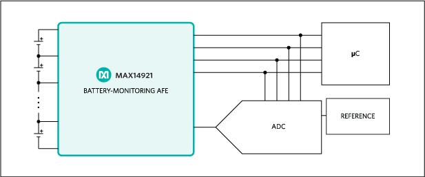
Figure 1. Accuracy-optimized architecture.
Architectural Analysis
From a design perspective, to obtain high accuracy, the microcontroller should factor as little as possible into the error of the overall system. While many microcontrollers feature internal ADCs and references, these generally do not have the required resolution or accuracy needed for reliable sub-millivolt measurements and should be avoided in applications that require such accuracy.
The accuracy-optimized architecture, shown in Figure 1, has the potential to provide the greatest accuracy of any of the architectures because it offers flexibility for individual selection of both the main components that contribute to system precision: the analog-to-digital converter (ADC) and the reference. Much like ADCs that are external to the microcontroller, references that are external to the ADC are more suited for high-accuracy systems. External references have better initial accuracy and temperature coefficient values than references internal to the ADC. This enhances both room temperature accuracy and accuracy over the whole operating temperature range of the system. By selecting an external reference and an ADC separately, however, additional cost is incurred, and the designer must marginally increase the price of the system as compared to other architectures to achieve the greatest accuracy.
Important Parameters
When selecting an ADC, integral nonlinearity (INL), offset and gain errors, and the temperature coefficients associated with offset and gain errors are the most significant aspects to which the designer will want to pay attention. The most important of these parameters is the offset error since it causes the most relative change in accuracy when compared with the other parameters. The gain error of the ADC is the second most important characteristic to select when looking for an ADC, followed by INL.
When selecting an external reference, initial accuracy and temperature drift are the two essential characteristics. An external reference that has excellent values for both of these parameters is essential to maintaining accuracy over the full operating temperature of the system.
In summary, the important design parameters associated with their respective component listed in order of importance are as follows:
- ADC
- Offset error
- Gain error
- Integral nonlinearity (INL)
- Gain-error temperature coefficient
- Offset-error temperature coefficient
- External Reference
- Initial output voltage accuracy
- Output voltage temperature coefficient
Entering the parameters listed above in the Total Error Calculations table of the Error Measurements spreadsheet (XLSX), available for download, produces an expected maximum six-sigma error over temperature as well as an expected maximum three-sigma error over temperature for the system. Using the calculated error as a guideline for meeting design requirements is advised, but actual accuracy is typically much better than even the three-sigma value, as seen in the component selection example below. See Appendix 2 for information on how to use the "Error Measurements" spreadsheet.
Component Selection/Example
Since accuracy is the main aim in this system, the designer must select system components accordingly. The MAX14920/MAX14921 require a capable microcontroller, an ADC with reasonably high resolution, and a solid voltage reference for optimum performance. A block diagram of the Maxim solution for maximum performance and high accuracy measurements using the MAX14921 can be seen below in Figure 2. A complete schematic, layout, and bill of materials can be found in the data sheet for the MAX14921 Evaluation Kit.
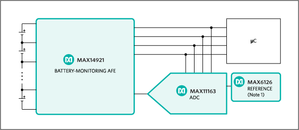
Figure 2. Maxim's evaluation kit solution for the MAX14921.
The quality of both the external ADC and the voltage reference make or break the accuracy of the system. The MAX14920/MAX14921 are capable of measurement accuracies well within 500µV of the battery voltage, and bench measurements have shown average measurement errors from the IC alone to be well under 300µV for most cell voltages (see the Typical Operating Characteristics in the MAX14920/MAX14921 data sheet). The resolution of the ADC and the accuracy of the reference in the Maxim solution have been selected to be high enough to allow for an LSB of less than 100µV. Maxim recommends the MAX1116316-bit ADC for its excellent offset error, gain error, and INL. For the external reference, Maxim recommends the MAX6126 reference for its low 0.02% initial accuracy and excellent temperature coefficient for reliable performance over the entire -40°C to +85°C temperature range. (Note 1)
A quick calculation using values from the data sheets for the MAX14920/MAX14921, MAX6126, and the MAX11163 along with the attached spreadsheet gives a six-sigma error of about 0.042% and a three-sigma error of about 0.027% for the complete Maxim solution. This translates to about 1.714mV maximum six-sigma error or 1.087mV maximum three-sigma error. When calculating errors from parameters given in IC data sheets, it is assumed that all errors are additive. In reality, errors can offset one another, thereby reducing the overall error of the system. As a result, the expectation is that the three-sigma system accuracy will be even better than 0.027%. Figure 3 shows actual cell measurements taken in the lab on the MAX14921EVKIT over temperature. Measurements were taken at various cell voltages and show a maximum change in error of only 0.009% (368µV) over temperature, with a maximum cell voltage measurement error of 0.017% (696µV).
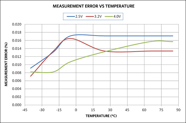
Figure 3. MAX14921 system measurement error over temperature.
When paired with the correct components in the accuracy-optimized architecture, the MAX14920/MAX14921 offer excellent accuracy. Maxim's recommended solution for high-accuracy battery measurement systems, the MAX14921EVKIT#, which includes the MAX14921, the MAX11163, and the MAX6126, features extremely low measurement error with solid performance over the extended -40°C to +85°C temperature range.
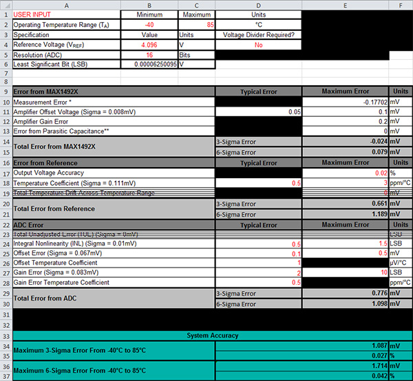
Figure 4. Error calculations for accuracy-optimized architecture.
Note 1: Some lithium cell chemistries have a full-charge voltage up to 4.4V per cell. For such chemistries Maxim recommends the MAX6194A reference. Cell B4 on the "Total Error Calculations" worksheet in the "Error Measurements" spreadsheet must be changed to 4.5V to account for the higher reference voltage.
Accuracy-Optimized, Cost-Reduced Architecture
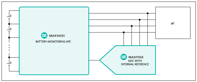
Figure 5. Accuracy-optimized, cost-reduced architecture.
Architectural Analysis
Cost-reduction needs often force designers to make the trade-off of reduced accuracy. This trade-off, however, need not greatly decrease system accuracy. A properly selected ADC with an on-board reference makes the accuracy-optimized, cost-reduced architecture shown in Figure 4 an excellent solution for systems requiring high accuracy within a budget.
This architecture still avoids use of the microcontroller's ADC to keep accuracy high, but it relies on an ADC with an internal reference. The reduction in component count in this architecture produces a reduction in cost, and while accuracy is diminished in a system with an internal reference as compared to an external reference, the trade-off is typically acceptable.
Important Parameters
Much of the important selection criteria for the characteristics of the components in the accuracy-optimized architecture also apply to this architecture. The main difference is that there is less flexibility with the reference parameters. As such, it is best to focus most attention on selection of the ADC's offset error, gain error, and INL parameters as well as the gain- and offset-error temperature coefficients. Since reference error and reference drift typically scale with the precision of the ADC's characteristics, it is not as important to rigorously assess these parameters, though it is always good to make sure they offer relatively good accuracy.
Overall, the most important design parameters associated with the accuracy-optimized, cost-reduced architecture listed in order of importance are as follows:
- Offset error
- Gain error
- Integral nonlinearity (INL)
- Gain-error temperature coefficient
- Offset-error temperature coefficient
Component Selection/Example
The accuracy-optimized, cost-reduced architecture eliminates the external reference, introducing the need for an ADC with an internal reference. The MAX11165 fits the bill for a high-accuracy system of this kind, offering offset error, gain error, and INL values equal to the MAX11163, while also including an internal reference with an initial accuracy of ±4mV with a temperature coefficient of 17ppm/°C maximum.
Again, using the "Error Measurements" spreadsheet attached to this application note shows that the maximum six-sigma error for this system is 0.178% (7.305mV) and the maximum three-sigma error for the system is just 0.122% (5.014mV). If anecdotal evidence from the actual performance of the MAX14921 Evaluation Kit serves as an indicator of true performance, this system should see much better performance than the maximum errors indicate. Note that such anecdotal evidence serves as a framework for a possible outcome, but actual system design should rely on maximum error.
While the cost-optimized architecture outlined above leads to a reduction in system accuracy, the trade-off does not have an overly negative impact on the accuracy of the system. In applications where such errors are acceptable, the MAX14920/MAX14921 battery-monitoring AFE, the MAX11165 ADC, and a capable microcontroller offer a lower-cost system with great accuracy.

Figure 6. Error calculations for accuracy-optimized, cost-reduced architecture.
Cost-Optimized Architecture
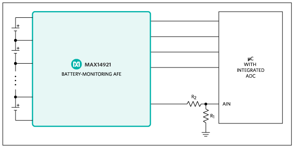
Figure 7. Cost-optimized architecture.
Architectural Analysis
Some battery-monitoring applications require cost and/or board space savings that necessitate a larger trade-off in accuracy than offered in the cost-reduced architecture above. For such applications it is best to eliminate all external components and use the ADC integrated with the system microcontroller. Using the ADC on board the microcontroller presents two difficulties in terms of accuracy:
- The on-board ADC typically has very low accuracy performance.
- A 3.3V microcontroller may have a reference around 1.195V. As a result, the integrated ADC can only accept a 1.195V full-scale voltage, but most cell-stack monitoring applications require a full-scale voltage of 4V or higher.
The first difficulty listed above is a trade-off that designers typically must accept, since the accuracy is determined primarily by the chosen microcontroller. The second problem requires a much more significant trade-off for the designer. To decrease the full-scale voltage at the input to the ADC a voltage-divider must be used. The converted value output from the ADC must then be multiplied by the IN/OUT ratio of the voltage-divider to regain the original scale. Multiplying the output magnifies the error caused by the first difficulty above, and the voltage-divider introduces error in three ways (discussed in the "Important Parameters" section below).
This architecture eliminates all peripherals and allows the MAX14920/MAX14921 to be implemented in space-constrained applications. Eliminating external components also decreases the cost of such a system, making this a viable cost-optimized solution or chemistries that do not require high precision measurement.
Important Parameters
When selecting a microcontroller, it is advised that at least one 12-bit (minimum) ADC be available for conversion of the output from the MAX14920/MAX14921. ADC characteristics typically scale with the cost of the microcontroller, so selecting a microcontroller within the budget is the most optimization needed here.
The resistor values are the most controllable parameter in this architecture. Consider an application with a maximum 4V cell voltage and a 1.195V reference on the ADC. The 4V input must be divided down to 1.195V to match the full-scale voltage capabilities of the ADC. Once the conversion is completed, the output value must then be multiplied by the IN/OUT ratio to regain the original 4V scale. In this case, the output must be multiplied by 3.35. The division of the input, conversion, and subsequent multiplication of the output introduces three sources of error.
The first form of error introduced by the voltage-divider is the error caused by imperfect resistor values due to calculated values being unavailable. For example, selecting R1 = 1MΩ requires R2 = 2.347MΩ. Such precise values are not available, so the designer must settle for a nearby value that is purchasable. In this case both 2.32MΩ and 2.37MΩ are available. It is advised to choose an actual value higher than the calculated value to keep the full-scale voltage of the divided signal below the 1.195V reference. If a value lower than the calculated value is selected, the full-scale voltage will exceed the reference causing loss of data. With R1 = 1MΩ and R2 = 2.37MΩ, neglecting all other factors, the voltage-divider introduces 8.05mV of error.
The second way that error is introduced through the voltage-divider is due to the tolerances of the resistors. Assuming 0.1% tolerance on both resistors, a maximum error of 1.67mV is introduced through the tolerances alone. When added to the error due to imperfect resistor values mentioned above, the total maximum error introduced can be as high as 9.73mV. The error increases quite a bit as the resistor tolerance is increased. If, for instance, the tolerance of both resistors is 0.5%, the maximum error due to tolerance increases to 8.4mV bringing the total maximum error due to imperfect resistor values and resistor tolerances to 16.39mV.
Lastly, the voltage-divider introduces error due to the need to multiply the output by the IN/OUT ratio. This error affects two areas:
- The errors introduced by the voltage-divider as mentioned above are introduced at the input to the ADC. This means that the error is included in the value output from the ADC. This value is then multiplied by the IN/OUT ratio. As such, the true error introduced at the output by the voltage-divider is the IN/OUT ratio (3.35 in this case) multiplied by the sum of the imperfect resistor error value and the maximum error due to resistor tolerance. In the above example, using 0.1% tolerance resistors, this means that the 9.73mV of error on the input becomes 9.73mV x 3.35 = 32.6mV on the output.
- The IN/OUT multiplier also amplifies the ADC and reference errors. Thus, if the total error introduced by the ADC and reference is 1mV, the error from the ADC after the multiplier is 1mV x 3.35 = 3.35mV.
Note: The high value of R2 = 2.37MΩ along with the 10pF (max) input capacitance to the ADC forms a RC time constant that must be accounted for in the system. Waiting 5 times the RC value, or about 120µs in this example, before beginning the ADC conversion allows the input capacitance to charge before sampling the signal.
Component Selection/Example
Since this architecture depends largely on which microcontroller is used, it is helpful to analyze a common, low-cost microcontroller. The Freescale Semiconductor K10P64M72SF1 is such a microcontroller. The integrated SAR ADC on the K10P64M72SF1 offers 12-bit single-ended conversions with a total unadjusted error (TUE) of ±6.8LSB (maximum). This corresponds to 6.8mV of maximum error from the ADC, which becomes 22.78mV of error after the output is multiplied by the IN/OUT ratio. The Freescale K10P64M72SF1 includes a 1.195V internal reference with a maximum 3.5mV reference error and a total 80mV reference temperature drift across the operating temperature range.
According to the "Error Measurements" spreadsheet, the MAX14920/MAX14921 and the on-board ADC of the Freescale K10P64M72SF1 produce a 12-bit output with a maximum six-sigma error of 251.307mV (861.17 LSB) giving a worst-case ENOB of 11.66 bits. The maximum three-sigma error is 116.849mV (400.42 LSB) and gives a minimum ENOB of 11.85 bits.
The cost-optimized architecture just outlined provides the designer with a large amount of cost reduction, yet still provides acceptable accuracy for systems using Lithium chemistries with moderate-to-steep discharge curves. This architecture offers the additional benefit of reduced footprint on a PCB, allowing design-in on a space-constrained application.
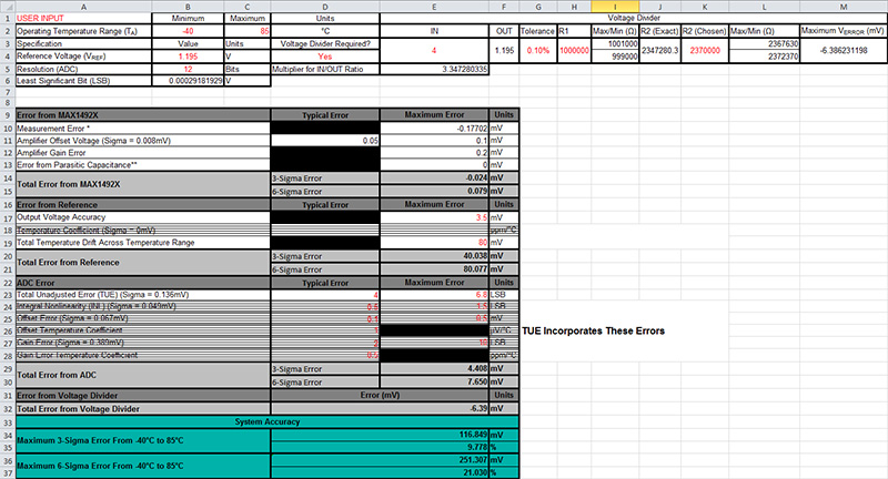
Figure 8. Error calculation for cost-optimized architecture.
Cost-Optimized, Accuracy-Enhanced Architecture

Figure 9. Cost-optimized, accuracy-enhanced architecture.
Architectural Analysis
The cost-optimized, accuracy-enhanced architecture takes the previously introduced cost-optimized architecture and improves accuracy by adding an external reference. The use of an external reference not only allows the designer to greatly reduce the inaccuracies due to the microcontroller's integrated reference, but it also decreases the amount by which the analog signal from the MAX14920/MAX14921 needs to be divided down. Since the IN/OUT ratio decreases with a higher voltage reference, the inaccuracies associated with that multiplying factor decrease as well. This offers large increases in accuracy even with a low-cost reference.
The addition of the external reference is the only differentiating factor between this architecture and the cost-optimized architecture mentioned above. Therefore, improved initial accuracy, lower temperature drift, and a lower IN/OUT ratio are the three advantages to this architecture over the cost-optimized architecture. The designer must decide if the increased cost of the system due to the external reference is sufficiently offset by the increased accuracy of this system.
Important Parameters
As discussed previously, the selection criteria for a microcontroller is that there be at least one 12-bit (minimum) ADC, and that the characteristics of the microcontroller's integrated ADC are acceptable for the desired system accuracy. The other parameter that affects accuracy is the selection of R1 and R2 in the voltage-divider. Refer to the "Cost-Optimized Architecture" section for analysis of the impact of the voltage-divider on the accuracy.
Selection of the external reference depends on the budget for the project as well as the capabilities of the microcontroller. Many microcontrollers operate off of a 3.3V supply, and only offer the capability to handle a 3.3V reference. For maximum accuracy, it is important to select a reference voltage as close to the full-scale input as possible while still operating within the capabilities of the microcontroller.
Other important factors for the voltage reference are the reference's initial accuracy and temperature coefficient. These factors are secondary, however, to selecting a reference voltage as close to the full-scale input as possible. The reason for this is to lower the IN/OUT ratio as much as possible and therefore decrease the amount the output must be multiplied on the output to regain the original scale. For example, with the internal voltage reference of the Freescale K10P64M72SF1 microcontroller, the IN/OUT ratio is 3.35, but using a 3.3V external reference produces an IN/OUT ratio of 1.21.
The improved IN/OUT ratio of the voltage-divider that comes with using a higher reference voltage coupled with the improved initial accuracy and temperature drift of an external reference make this architecture a great cost-reduced architecture for applications requiring higher accuracy than the cost-optimized architecture previously discussed while still keeping cost low.
Component Selection/Example
The Freescale Semiconductor K10P64M72SF1 microcontroller can again be used in this example. Using the same microcontroller as well as 0.1% tolerance resistors make the accuracy analysis of this system simple. The MAX6034B voltage reference, with 13mV initial accuracy and 75ppm/°C (max) temperature drift offers great performance at low cost (Note 2). The MAX6034B also has a 3.3V option that the selected microcontroller will accept, and which greatly improves accuracy over a 1.195V reference as used in the cost-optimized example above. The 3.3V reference allows the IN/OUT ratio to be just 1.21.
The voltage-divider must now divide the 4V maximum voltage from the battery-monitoring AFE down to 3.3V. Selecting R1 = 1MΩ yields a calculated resistor value of R2 = 212.121kΩ. Since 210kΩ and 213kΩ resistors are the closest available, the 213kΩ resistor will be selected to avoid exceeding the reference voltage at full-scale. With these resistor values on the voltage-divider, the maximum error introduced by the voltage-divider is 3.55mV.
The K10P64M72SF1 microcontroller's internal ADC offers accuracy of 6.8 LSB, and with the MAX6034B as the external reference this system achieves six-sigma error as low as 31.154mV and three-sigma error as low as 17.632mV. As compared to the cost-optimized architecture discussed above, the cost-optimized, accuracy-enhanced architecture in this example offers an 87.6% decrease in maximum six-sigma error with only a minor increase in the cost of the system.
Note 2: For a low-cost 3.3V voltage reference with higher accuracy than the MAX6034B, Maxim recommends the MAX6034A voltage reference.
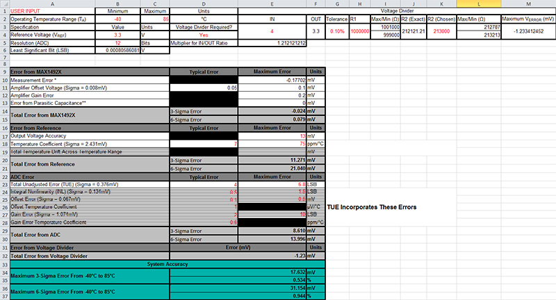
Figure 10. Error calculations for cost-optimized, accuracy-enhanced architecture.
Conclusion
The architectures outlined above give system designers flexibility in implementing battery-management systems. No matter the end-application and design constraints, the MAX14920/MAX14921 offer a flexible design capable of delivering high-performance battery monitoring and cell-balancing capabilities that fit multiple design constraints. The performance of the MAX14920/MAX14921 can be tuned to specific applications simply by the proper selection of the surrounding building blocks.
Appendices
Appendix 1 - Layout Matters
Good layout techniques are required for optimal results. These topics, however, are out of the scope of this application note. See the MAX14921EVKIT data sheet and application note 5495, "PCB Layout Guidelines for the MAX14921 High-Accuracy 12-/16-Cell Measurement AFE" for more details on layout and board design.
Appendix 2 – Calculating Error Using "Error Measurements" Spreadsheet
The Error Measurements spreadsheet is intended to assist designers in estimating the total error of a system based on maximum errors introduced by individual components. The spreadsheet contains two worksheets with one aimed at calculation of error introduced by the MAX14920/MAX14921 battery-monitoring AFE given timing and component selection, and the other aimed at calculation of the maximum three- and six-sigma errors of the entire system. It is best to begin by using the "MAX1492X Error Calculations" worksheet as it factors into the total error of the system.
MAX1492X Error Calculations Worksheet
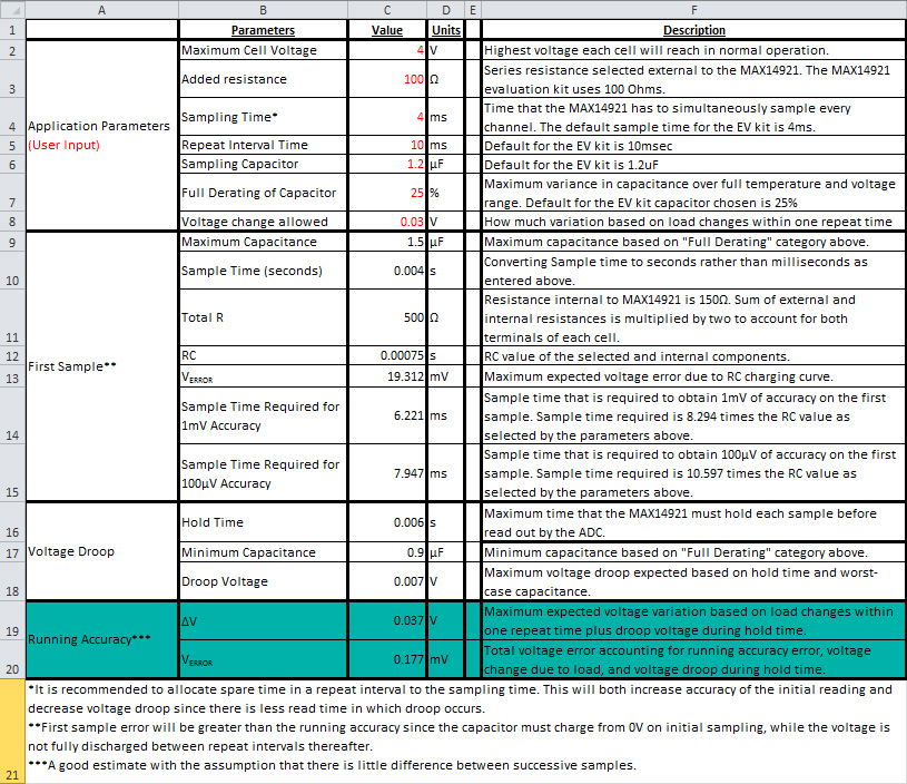
Figure 11. MAX1492X error calculations worksheet.
To calculate the error introduced by the MAX14920/MAX14921, simply fill in cells C2 to C8 with the data corresponding to the respective parameter in column B. The descriptions offered in column F provide more detailed information as to what data is required.

Figure 12. Rows 2 to 8.
Once all of the information is provided, the equations contained in the cells from row nine down to row twenty do the rest of the work. The purpose of these calculations is to account for different sources of error that are introduced through design decisions on the MAX14920/MAX14921. The RC time-constant of the added resistance along with the sampling capacitors requires sampling time to be allowed. If the capacitor is not allowed to charge to a sufficiently high value due to a lack of sampling time and/or too high of an RC time constant, the accuracy of the system will diminish. A voltage droop can also occur if the hold time of the system is too large as the capacitor will begin to discharge through the parasitic resistances and the voltage will drop slightly across the capacitor.
The calculations on this worksheet show the voltage droop due to the hold period (cell C18), the total voltage error due to droop and load changes within a charging interval (cell C19), and the total running error of the system (cell C20). The running accuracy of the system will always be negative due to the fact that the capacitor cannot charge above the battery's cell voltage. Note that the running accuracy assumes that there is little time or voltage variation between successive samples. First sample accuracy (cell C13) is more accurate for systems with large intervals between successive samplings or with large variations in voltage between samples as it assumes that the capacitor is discharged by the time the next sampling time begins.
There are four application parameters that deserve special mention and explanation: sampling time, repeat interval time, hold time, and full derating of capacitor.
Repeat Interval
The repeat interval of the system is the interval between ADC conversion cycles. If the ADC begins a new conversion every 10ms, then the repeat interval is 10ms. The repeat interval consists of the sampling time and the time allocated to the conversion of all 16 channels by the ADC.
Sampling Time
The sampling time of the system refers to the period of time within a repeat interval that is allocated to allowing the sampling capacitors used with the MAX14920/MAX14921 to charge. It is recommended that as much time as practical be allocated to the sampling time within a repeat interval. Increasing the sampling time improves the error of the system by reducing the voltage error due to the charging curve of the RC circuit as well as by reducing the voltage droop that occurs during hold time.
The Error Measurements spreadsheet calculates the sampling times required for either 1mV or 100µV accuracy in cells C14 and C15, respectively.
Hold Time
The hold time is the maximum time the sampling capacitor must hold the sampled voltage before the ADC begins conversion on that channel. The last channel converted by the ADC will have the longest hold time, and consequently the largest voltage droop. It is important that the conversion sequence go from the cell with the highest voltage with respect to ground to the lowest voltage with respect to ground as leakage current will scale with this absolute voltage. Sequencing this way reduces the voltage droop on the highest voltage cell.
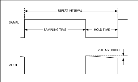
Figure 13. Timing diagram.
Full Derating of Capacitor
The full derating is the expected variance in capacitance due to temperature, voltage, and tolerance of the selected capacitors. This parameter varies with dielectrics, temperature ranges, and maximum cell voltage of a system, so this is the responsibility of the system designer to estimate. The estimate for the MAX14921 EV kit, which uses X7R capacitors, a maximum cell voltage of 4V, and has a -40°C to +85°C temperature range, is 25%.
Total Error Calculations Worksheet
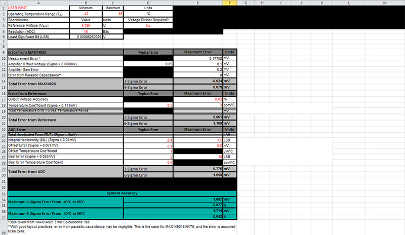
Figure 14. Total error calculations worksheet.
Using the Total Error Calculations worksheet on the Error Measurements spreadsheet is straightforward. The top left of the worksheet (below) asks for the specifications of the application. The operating temperature range should be entered into cells B2 and C2, the voltage reference value should be entered into cell B4, and the resolution of the ADC should be entered into cell B5. Cell B6 has an equation to calculate the LSB of the system from the entered values. Note that if a different reference value, such as 1.195V or 3.3V in the examples above or 4.5V when using lithium chemistries other than lithium-phosphate, cell B4 should be changed to the reference value used.

Figure 15. Application-specification cells.
If the application requires a voltage-divider to decrease the full-scale voltage, use the pulldown menu in cell D4 to select "Yes". This causes additional cells to appear, and parameters for the voltage-divider can be entered in the new cells (pictured below). Simply enter the system's maximum cell voltage in cell E3, the value chosen for R1 into cell H3, and the tolerance of the resistors into cell G3. The spreadsheet automatically obtains the "OUT" value in cell F3 from the Reference Voltage cell (B4). Once this data has been entered, the equation in cell J3 will give the calculated R2 value. Based on availability, the chosen R2 value will be different from the calculated value. The actual value should be entered into cell K3, and when that is done, cell M3 outputs the maximum error introduced by the voltage-divider. This value may be negative, reflecting the fact that the error introduced by the voltage-divider causes error below the maximum reference value. The voltage-divider error value is automatically calculated by cell E32 and entered into the final calculation.

Figure 16. Voltage-divider error calculator.
The bottom section of the "Total Error Calculations" worksheet allows the user to enter the relevant characteristics from each component into the spreadsheet (Figure 17). Each section has relevant specifications for each component as described above. Because there are many approaches to specifying error in particular instruments, there are multiple options for each section. Each category of data has a pulldown menu in column F to allow change of units. For instance, cell F17 allows the user to select percent accuracy or accuracy as measured in mV depending on how the data sheet specifies this characteristic (Figure 18).
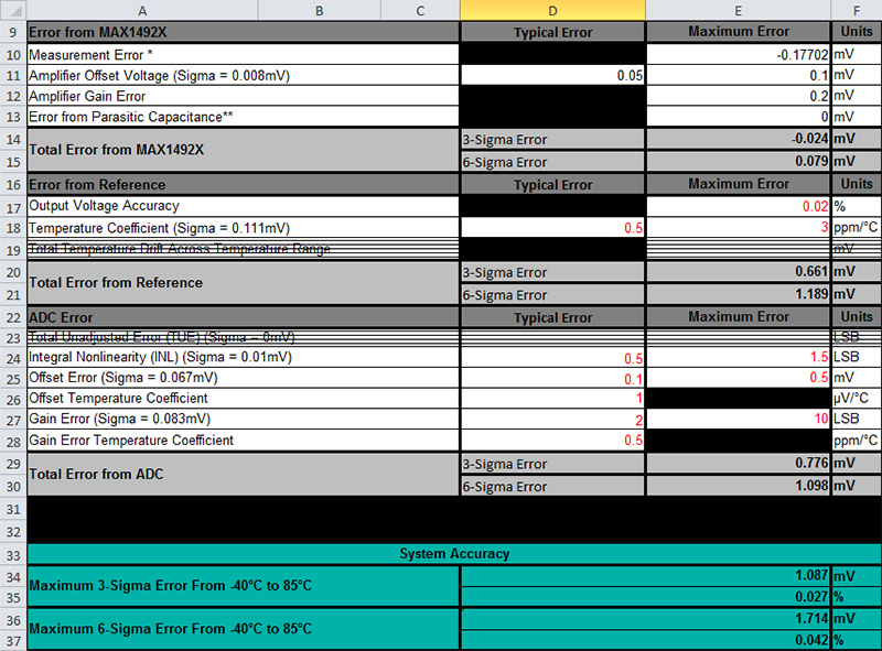
Figure 17. Component error calculations.

Figure 18. Selecting unit of measurement.
The "Error from Reference" section and the "ADC Error" section contain cells with lines through the row depending on the values in the cells in the same section. This is to indicate that when one value is entered, another is ignored. In the "Error from Reference" section, the "Temperature Coefficient" and "Total Temperature Drift Across Temperature Range" sections are mutually exclusive. If one value is non-zero, the other is crossed out as seen in Figure 19.

Figure 19. Mutually exclusive parameters.
If both the "Temperature Coefficient" and "Total Temperature Drift Across Temperature Range" cells have non-zero values in them, an error message will appear to the right of the cells indicating that only one value can be used.

Figure 20. Mutually exclusive parameters error message.
In the "ADC Error" section, the user can either enter the individual DC accuracy specifications (Offset Error, INL, etc.) or the user can enter the total unadjusted error (TUE) in the top cell if the data sheet offers this parameter. If the user enters a non-zero TUE value, the individual parameters are ignored, the cells become crossed out, and a dialog explaining that TUE covers the parameters that have been crossed out appears as pictured in Figure 21.

Figure 21. Total unadjusted error message.
With all of the data entered in each section, the equations in the "System Accuracy" section provide both the maximum six-sigma error over temperature as well as the maximum three-sigma error over temperature. With these values, the designer can make educated decisions on what components produce the desired accuracy for a given application.
This spreadsheet is intended to aid the designer in building a system that meets specific needs, but it is important to note that proper layout and other factors also play a key role in system performance. This spreadsheet should not be viewed as the final authority, but as a useful tool that can offer insight into what accuracy can be expected before prototyping begins.

Figure 22. Component error calculations.

