
Getting Started with a Scalable, X-Band AESA Tile
Key Takeaways
|
Abstract
A new highly integrated, scalable X-band (8GHz to 11GHz) phased-array platform is built on a tile-based architecture, ranging from a single 16-element beamforming tile to a fully digitized 64-element hybrid array. This practical getting-started guide surveys the product family and describes hardware setup and connectivity, subsystem integration, power sequencing, thermal considerations, control and initialization, calibration and beam steering, and software operation.
Product Family Overview
The ADSY2301 is a highly integrated active electronically steered array (AESA) designed to support scalable aperture configurations for advanced sensing and communication applications. At its core, the system features a 4 × 4 uniform rectangular array (URA) of linearly polarized elements spaced at one-half wavelength (λ/2) referenced to 11GHz, paired with integrated transmit/receive (Tx/Rx) modules and beamforming integrated circuits (BFICs), enabling operation across 8GHz to 11GHz.
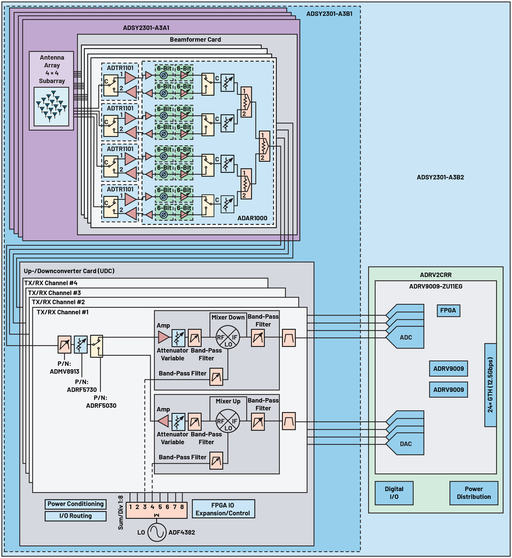
The product family scales through a tile-based approach to meet a range of evaluation needs as shown in the block diagram in Figure 1.
- ADSY2301-A3A1: A single 4 × 4 URA beamforming tile (16 elements) operating directly at the 8GHz to 11GHz RF band with no onboard frequency conversion.
- ADSY2301-A3B1: A 2 × 2 arrangement of four tiles (8 × 8 URA, 64 elements) integrated with an up-/downconverter (UDC) for frequency conversion, local oscillator (LO) generation, power regulation, and local FPGA control. Referenced herein as a quad-tile.
- ADSY2301-A3B2: The hybrid array is an integrated development platform comprising a quad-tile, an ADRV9009-ZU11EG digitizer SOM, and an ADRV2CRR-FMC carrier card mounted on a mechanical chassis. This offering is intended for rapid prototyping in a laboratory environment; the integrated solution is not intended for field deployment.
- ADSY2301-KIT1/KIT2: Evaluation kits supporting the beamformer/ antenna hardware with breakout boards, digital cable requirements, power cable assembly, and a board support package for a Xilinx® ZCU102 control platform.
For product and evaluation-platform offerings and ordering options, see the ADSY2301 data sheet and user guide.
Hardware Setup and Connectivity
Interfaces
RF connections between the antenna and beamformer cards are made through SMPM bullet connectors (16 per tile, 64 on the quad-tile). On the hybrid array, eight SMPM-to-U.FL RF cables route the converted IF between the quad-tile and the digitizer. Digital control, power, and data interfaces connect the beamformer cards, UDC, and control platform. For net names, pin-level definitions, and connector interface detail, refer to the ADSY2301 interface control document (ICD).
Required External Equipment
To fully evaluate the platform, additional RF and test equipment is needed that is not included with the ADSY2301 purchase.
- Host FPGA: For the single tile or the quad-tile, the user provides the host FPGA; the recommended board is the Xilinx ZCU102 evaluation board, for which supported drivers are provided. For the hybrid array, the ADRV9009-ZU11EG acts as the host.
- Reference Clock: There is an option to provide an external reference clock to the system, ideally the common reference for all RF equipment used during evaluation. A 122.88MHz crystal is available for an onboard reference.
- Power Supplies: For the single tile, a power supply able to generate +4V, –6V, and +5.7V and a 16V to 28V rail are needed. The quad-tile requires a 28V power supply, whereas the hybrid array requires a 28V and 12V power supply.
Subsystem Integration
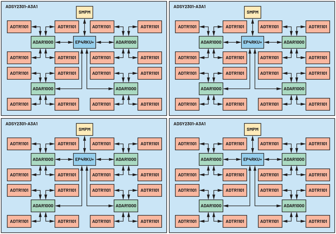
The ADSY2301 integrates several RF and digital subsystems into a single phased-array platform. Understanding the role of each subsystem supports initial bring-up and later scaling. A block diagram of the quad tile system components is shown in Figure 2.
Beamformer Tile
The beamformer card services the sixteen elements of a tile through four ADAR1000 4-channel BFICs, arranged as a 2 × 2 grid with each BFIC driving a local 2 × 2 element quadrant. The card also carries the per-element ADTR1101 transmit-receive modules (TRMs) between the BFICs and the antenna elements.
Up-/Downconverter (UDC)
The UDC performs RF-to-IF conversion and generates the LO. The LO is produced by an ADF4382 synthesizer. Receive downconversion uses a highly integrated microwave downconverter IC, and transmit upconversion is done with a highly integrated microwave upconverter IC. Band-pass filtering is provided by the ADMV8913 tunable filter. The UDC also provides power regulation and control aggregation for all 64 channels via a local power distribution network and onboard FPGA.
Integrated Quad-Tile Development Platform
On the hybrid array, the ADRV9009-ZU11EG and ADRV2CRR-FMC carrier card provide data conversion and the digital back end, supplying four transmit and four receive channels across the full 64-element aperture.
Scaling and System Modularity
The architecture scales through a tile-based approach. A 2 × 2 arrangement of single tiles forms the quad-tile, an 8 × 8 (64-element) URA. The element pitch and 8GHz to 11GHz operating band are preserved across tile boundaries, so the aperture scales without changing per-element spacing. The four tiles mount to a common plate and interface to the UDC, which provides frequency conversion, LO control, power regulation, and control aggregation for all 64 channels.
The platform is modular at each layer, including the antenna, beamformer card, converter, and control/digitizer. This modularity allows each configuration to match the evaluation objective, from a standalone tile to the fully digitized 64-element hybrid array. A future article will cover additional scaling considerations.
Power Rails and Sequencing
Correct power-on ordering protects the BFICs and the transmit/ receive modules. A key principle across all configurations is to pinch off the amplifier gates during initialization of the ADAR1000s. The degree of automation differs by offering. On the quad-tile and hybrid array, the supplied initialization scripts manage most of the sequence through the UDC, whereas a standalone tile is sequenced manually by the user.
Supply Rails
The system uses several supply rails, including +4V and –6V (beamformer), 5.7V (receive), and a 16V to 28V power-amplifier drain (transmit). The UDC additionally distributes +5.0V, +3.3V, and –2.5V/–3.3V rails on converter-equipped builds.
Standalone-Tile Power Sequencing
- Power on the +4V and –6V rails.
- Power on the ZCU102 or ADRV9009-ZU11EG, depending on product offering.
- Initialize the ADAR1000s and set pinch-off values for the low-noise amplifiers (LNAs) and power amplifiers (PAs).
- Ensure the bias DAC mode is set to On and the transmit/receive source is set to SPI.
- For receive operation, power on the 5.7V supply.
- For transmit operation, power on the drain-voltage supply (16V to 28V).
- If using an external transmit/receive signal, set the bias DAC mode to toggle and the transmit/receive source to external (required for transmit operation).
Quad-Tile and Hybrid-Array Power Sequencing
On the quad-tile, the UDC regulates and distributes power to the rest of the system through an analog and digital sequence. The sequence verifies that each power rail is enabled correctly and aborts if an error occurs at any stage. The hybrid array uses the same sequence with the ADRV9009-ZU11EG as the primary controller in lieu of the ZCU102.
Thermal Monitoring and Duty-Cycle Management
Each ADAR1000 includes an integrated temperature sensor, providing 16 sensors across the 8 × 8 URA of the quad-tile. These sensors can be leveraged to monitor array temperature and maintain device junction temperatures within the specified limits. During transmit operation, duty cycles above 35% may cause the devices to approach the junction-temperature limit.
To maintain adequate thermal margin, enable transmit/receive pulsing through either an external pulse generator or the FPGA’s internal time division duplexing (TDD) control engine. As a quick validation, monitoring the PA VDD current specified in the ADTR1101 data sheet can help confirm that the current increase when transmit elements are enabled scales proportionally with the transmit/receive pulse duty cycle.
Control Modes and System Initialization
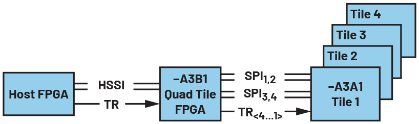
The front-end BFICs and TRMs are controlled through an SPI interface and an external transmit/receive control signal. The ADAR1000 beamformers support two methods for switching between transmit and receive: SPI-controlled switching, in which software manages the transmit/receive state directly, and external transmit/receive-pin control, in which a single hardware signal drives the state (low = receive, high = transmit). The system uses positive switch logic and is propagated as a copy of the host FPGA-generated signal. The evaluation software applies the selected control mode and associated switch-logic settings during initialization. Figure 3 shows a diagram of the primary control serial links for transmit/receive pulsing of the ADSY2301.
Bring-up is handled by the initialization script, which connects to the control platform, applies the FPGA device-tree overlay (on the ZCU102 kit), configures the ADAR1000 beamformers, and sets the PA/LNA bias. Example initialization scripts can be found in the Python repository under the examples/adsy2301_examples folder.
For the SPI and transmit/receive electrical interfaces and the connector and pin-level definitions, refer to the ADSY2301 ICD; for the complete ADAR1000 register map, refer to the ADAR1000 data sheet.
Element Indexing, Calibration, and Beam Steering
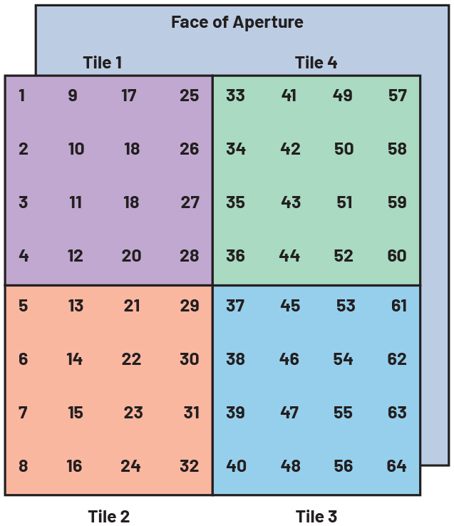
The ADSY2301 references per-element linear indexing to provide a consistent command-and-control framework for both single-tile and quad-tile configurations. Each tile contains 16 elements arranged in a 4 × 4 column-major map, with element 1 at the upper left. The quad-tile extends this convention to an 8 × 8, 64-element map. Figure 4 shows the per-element linear indexing for the quad-tile array.
Calibration matches the phase and gain of all array elements using the variable amplitude and phase (VAP) controls integrated into the ADAR1000 BFICs. A separate article will cover the calibration procedure in detail.
Beam steering applies amplitude and phase weights to each element according to the logical numbering used by the control software. The calibration and steering scripts operate on these element indices. After the array is calibrated at the operating frequency, the ADAR1000 class can steer it to a specified angle.
Calibration and beam-steering examples are available in the Python repository under examples/adsy2301_examples.
Software Setup and Control
The ADSY2301 can be operated through an open-source libiio and Python software stack. PyADI-IIO abstracts device control and supports scalability from a single tile to the full 64-element array. Installation instructions are available in the PyADI-IIO system-level documentation.
The abstraction makes basic electronic-steering examples (receive or transmit) straightforward, and provides a foundation for more advanced applications such as pulsed operation and simultaneous transmit/receive operation.
Conclusion
The ADSY2301 integrates the RF, beamforming, frequency-conversion, power, control, and digitization functions required to evaluate X-band phased array systems. Its tile-based architecture supports a common development approach across configurations ranging from a 16-element beamforming tile to a 64-element hybrid array. The Python and libiio software stack further provides a consistent interface for initialization, configuration, calibration, and electronic beam steering.
The hardware and software procedures described in this article establish a repeatable workflow for progressing from initial setup and power-on to controlled array operation. This foundation supports subsequent over-the-air calibration, beam-pattern characterization, performance optimization, and extension to larger apertures.
The technical article “Practical Beam Steering Using a Modular X-Band Phased Array” presents the calibration process and measured performance of the single-tile and quad-tile configurations.