
Practical Beam Steering Using a Modular X-Band Phased Array
Key Takeaways
|
Abstract
This article demonstrates practical beamforming performance using both single-tile and multi-tile array configurations. Measurements include embedded element characterization, over-the-air calibration, beam steering validation, and scaling from a single-tile 4 × 4 element array to a multi-tile 8 × 8 element array.
Results demonstrate excellent channel-to-channel amplitude and phase consistency, enabling accurate beam steering, low beam-pointing error, and scalable array performance with minimal calibration overhead.
Beamforming Fundamentals
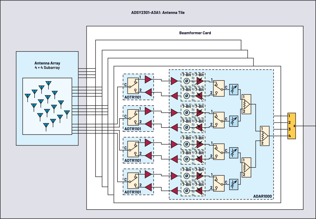
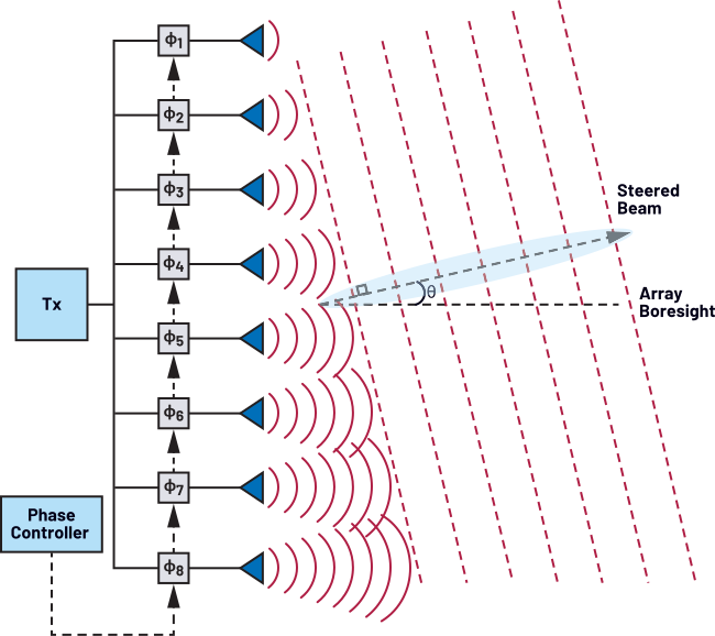
The ADAR1000 beamforming IC (BFIC) provides independent phase and amplitude control for each antenna element, enabling precise electronic beam steering. Phase control is implemented with 7-bit resolution (2.8° LSB), while amplitude control is implemented with 7-bit resolution (≤0.5dB LSB).
The ADTR1101 transmit/receive module (TRM) serves as the RF front-end for each element path, providing high transmit power, low-noise receive capability, and integrated transmit/receive (Tx/Rx) switching.
Figure 1 shows a block diagram of the analog beamforming architecture of the ADSY2301 tile. Figure 2 shows how the phase shifter can be used to electronically steer the beam.
Measurement Approach
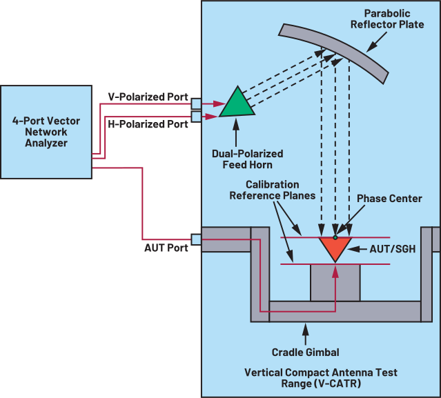
The ADSY2301 was measured inside a vertical compact antenna test range (Keysight V-CATR). A calibrated standard gain horn (SGH) with error of ±0.2dB is used to calibrate the chamber itself. The chamber calibration establishes an RF reference plane at the antenna aperture, enabling accurate measurements of realized gain and beamforming performance. Figure 3 shows a block diagram of the V-CATR measurement setup with the RF calibration planes shown.
Phase Center Alignment
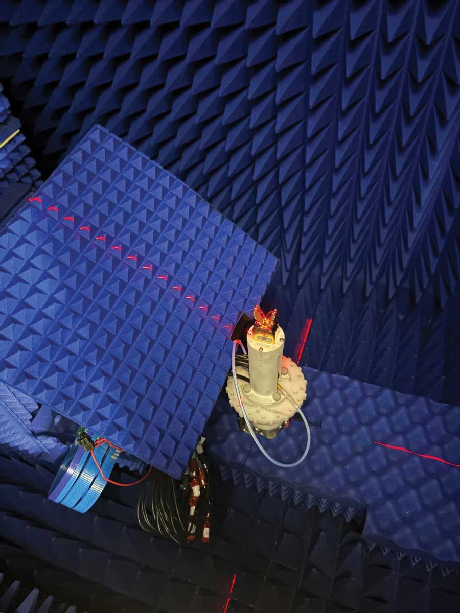
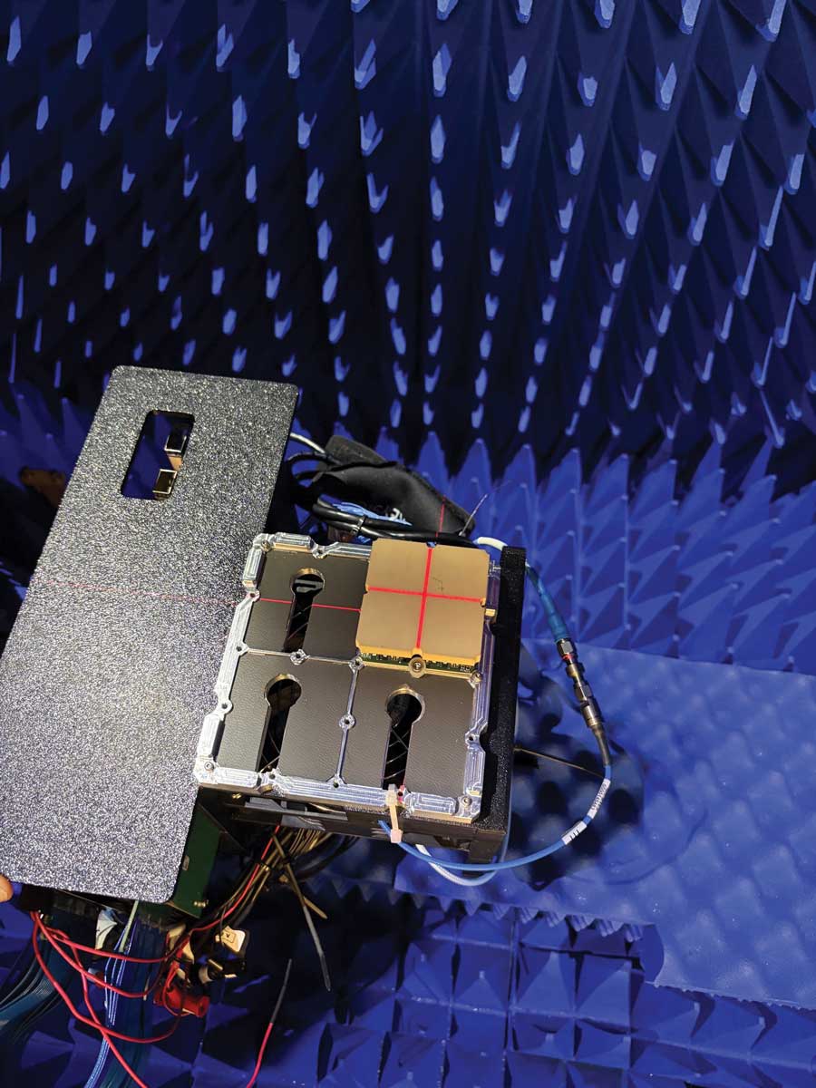
An important consideration when calibrating over-the-air (OTA) is to make sure the phase center of the SGH is physically located at the same phase center as the antenna under test (AUT). Mechanical alignment fixtures and laser positioning tools were used to ensure repeatable phase-center registration between the SGH and AUT after installation on the positioner, as shown in figures 4 and 5.
Chamber Calibration Procedure
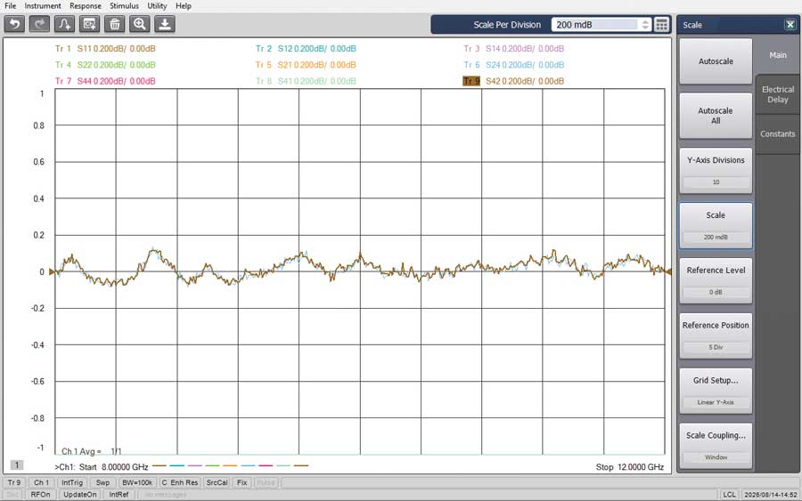
A gain-transfer calibration method was used to characterize the compact range. The calibrated SGH served as the gain reference standard. During calibration, the effects of free-space path loss, feed-chain losses, and residual chamber errors were removed from the measurement system. The resulting correction factors were applied to subsequent AUT measurements to enable accurate realized-gain extraction across the operating frequency range.
Figure 6 shows the residual chamber calibration error after application of the gain-transfer correction. The overall error is within ±0.2dB.
Calibration Procedure
Although the ADSY2301 exhibits excellent inherent channel matching, an optional OTA calibration procedure was performed to evaluate the maximum achievable beamforming performance. The objective is to equalize amplitude and phase across all element channels prior to beam steering.
- Set the amplitude of each channel BFIC VGA to maximum and set the phase shifters to their minimum.
- Turn on each channel individually and measure amplitude and phase.
- Select the lowest-power channel as the amplitude reference. Calculate the offsets needed on other channels’ VGAs to match the lowest amplitude and then apply the offsets.
- Select any channel as the phase reference. Calculate the offsets needed on other channels’ phase shifters to achieve phase alignment and apply the offsets.
- Verify by measuring amplitude and phase across all 16 channels.
Following calibration, residual channel-to-channel errors are typically limited by the finite resolution of the amplitude and phase control circuitry. After calibration, the boresight pattern can be measured to verify quality.
Embedded Element Characterization
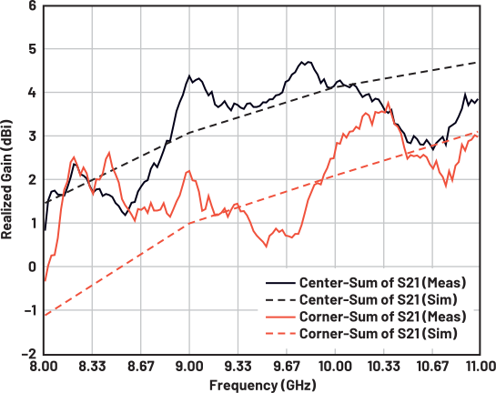
While conventional element-by-element calibration provides excellent results, embedded element measurements provide additional insight into mutual coupling and finite-array interactions. The embedded element pattern represents the radiation response of an individual antenna while all neighboring elements remain present in the array environment. Edge elements experience a different electromagnetic environment than center elements due to finite-array effects.
Figure 7 shows the measured realized gain of a center element and a corner element of the ADSY2301-A3A1. They match closely with simulation and highlight the finite-array effect.
Array-Level Receive Gain
Following channel equalization, the receive performance of the complete 4 × 4 tile was evaluated across the 8GHz to 11GHz operating band. Figure 8 shows the measured co-polarized and cross-polarized receive gain at boresight.
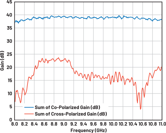
The measured cross-polarization isolation exceeds 20dB across most of the operating bands and remains better than 16dB throughout the entire frequency range.
Single-Tile Beamforming
Following calibration, the ADSY2301-A3A1 4 × 4 tile was configured to electronically steer beams across the visible scan region. Far-field measurements were then collected to validate beam-pointing accuracy, gain performance, and pattern quality. The gimbal in the V-CATR automatically moves the AUT while measuring received complex power at each angle to build 2D and 3D radiation pattern plots for each beam state.
Figure 9 shows uncalibrated far-field patterns while scanning from –60° to +60° in 15° steps. Figure 10 shows calibrated far-field patterns at those same scanning states.
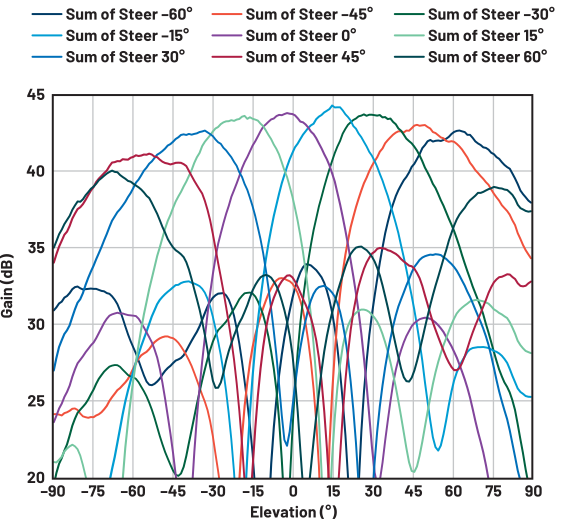
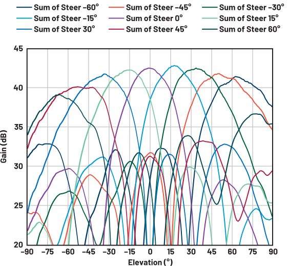
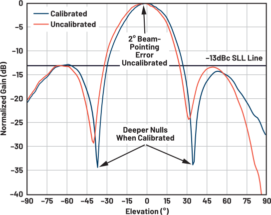
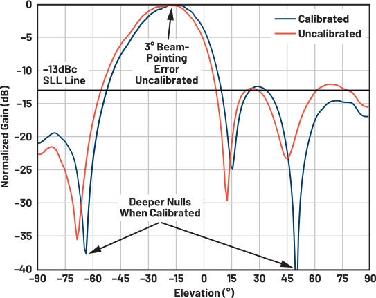
The small difference between calibrated and uncalibrated operation demonstrates the inherent phase and amplitude consistency of the architecture. Figures 11 and 12 show normalized comparisons between calibrated and uncalibrated beam states. Calibration introduces a small reduction in peak realized gain due to channel equalization while improving beam-pointing accuracy, null formation, and pattern fidelity.
Scaling to Multi-Tile Arrays
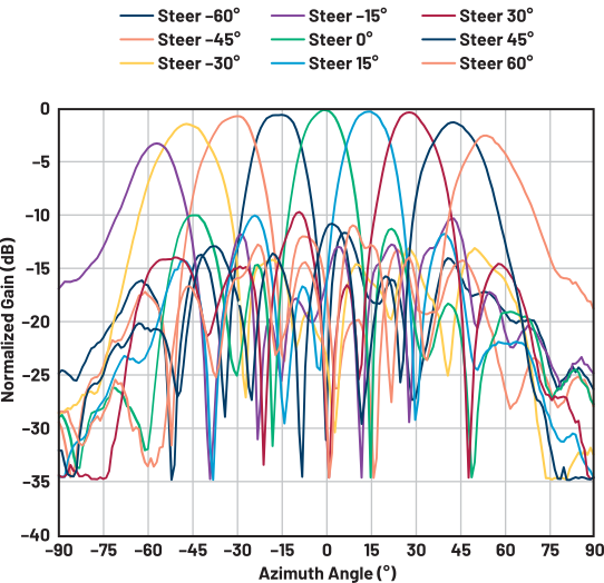
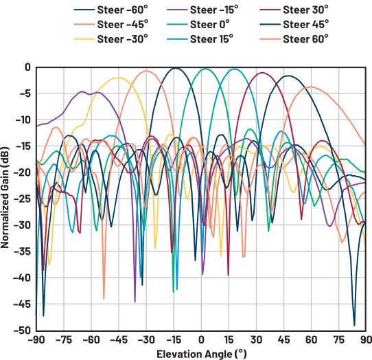
Scaling from a single 4 × 4 tile to a four-tile 8 × 8 array demonstrates the modular architecture of the platform. The larger aperture provides increased directivity, higher effective isotropic radiated power (EIRP), narrower beamwidth, and improved scan performance at wide steering angles. The OTA calibration workflow used for the single-tile configuration is repeated for the 8 × 8 array. The resulting measurements verify that beamforming performance scales predictably as additional tiles are integrated into larger apertures. Figures 13 and 14 show the horizontal and vertical beam scanning patterns for the four-tile 8 × 8 array.
Pulsed Radar Capabilities
In addition to continuous-wave (CW) beamforming operations, the ADSY2301 architecture supports pulsed radar applications through the integrated ADAR1000 BFICs and ADTR1101 TRMs. Pulsed operation enables high peak transmit power while reducing average power consumption and thermal loading. Key performance metrics include pulse amplitude stability and transmit/receive switching speed.
To evaluate pulsed operation, the ADSY2301 was configured for a 2μs transmit interval followed by an 8μs receive interval, corresponding to a 20% transmit duty cycle. Measurements were performed to characterize output power stability during the transmit pulse and to verify the transition time between transmit and receive modes.
Figure 15 shows the measured pulsed transmit response of the ADSY2301 operating at 2W output power per element. The network analyzers’ CW-time mode captures the output power throughout the duration of the transmit pulse, enabling evaluation of gain stability.
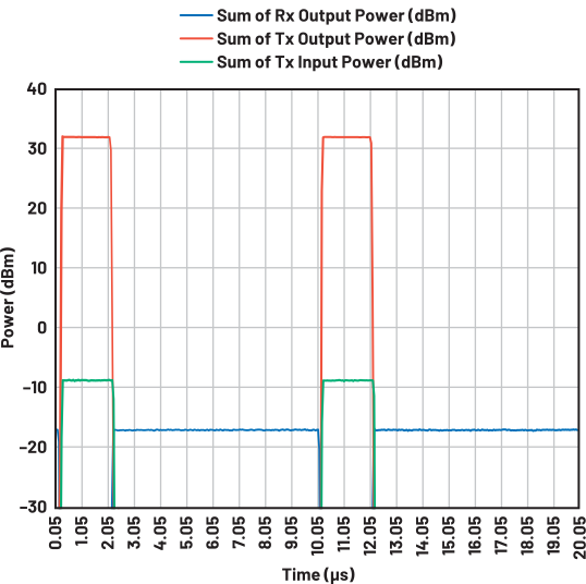
The measured output power variation was approximately 0.11dBm over the 2μs transmit pulse, demonstrating excellent pulse fidelity and output-power stability. A 150μs transmit pulse will see a drop of approximately 0.7dBm.
Rapid transition between transmit and receive operation is an important metric for pulsed radar systems. Fast transmit/receive switching minimizes receiver blind time after transmission and maximizes available receive time for target observation.
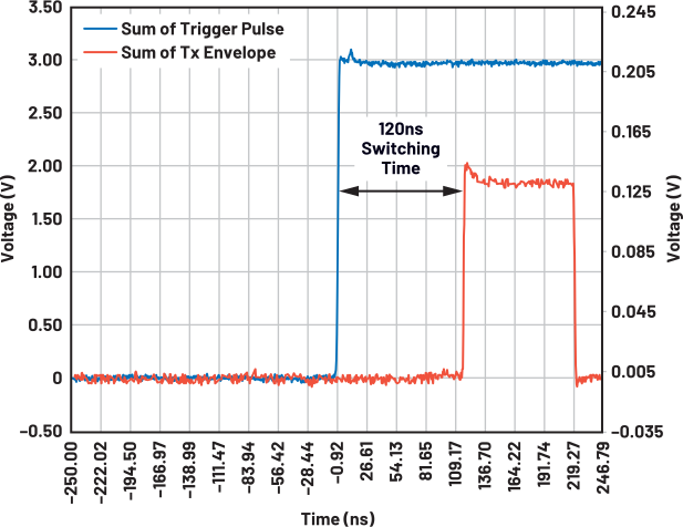
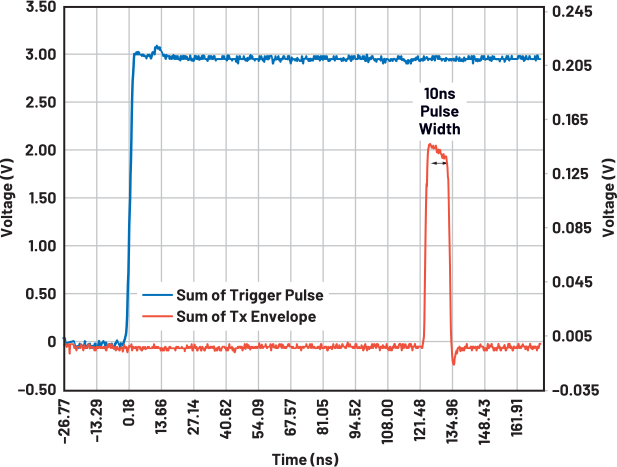
To characterize switching performance, a directional coupler was inserted into the transmit signal path and monitored using an envelope detector connected to an oscilloscope. This measurement captures the transmit pulse envelope and allows the transition between transmit and receive states to be directly observed.
Figure 16 shows the measured transmit pulse envelope and transmit/receive switching response. The measured transmit-to-receive switching time was approximately 120ns, demonstrating the ability of the architecture to support pulsed radar operation with short recovery times and high-pulse-repetition frequencies.
Key Performance Observations
- Accurate electronic beam steering demonstrated from –60° to +60°.
- Embedded element measurements closely matched simulation.
- Excellent channel-to-channel amplitude and phase consistency observed prior to calibration.
- OTA calibration improved beam-pointing accuracy and pattern fidelity.
- Single-tile and multi-tile measurements showed predictable scaling behavior.
- The modular architecture enabled seamless expansion from a 16-element array to a 64-element array.
Conclusion
The ADSY2301 was developed to provide a scalable building block for X-band phased array systems, allowing developers to evaluate, prototype, and deploy electronically steered apertures without the complexity of a custom array design.
The measurements presented throughout this document demonstrate how it can be used as both a standalone 16-element beamforming tile and as part of a larger multi-tile phased array. Chamber-calibrated measurements verified accurate beam steering from –60° to +60°, while embedded element characterization and OTA calibration demonstrated the strong amplitude and phase consistency achieved across element channels.
For customers developing larger apertures, the transition from a single 4 × 4 tile to a four-tile 8 × 8 array showed predictable beamforming performance and straightforward scalability using the same beam steering and calibration methodology. The small difference between calibrated and uncalibrated measurements further illustrates the level of channel matching inherent to the architecture, reducing the calibration burden often associated with phased array systems.
Beyond CW beamforming operation, pulsed measurements demonstrated stable transmit performance, low pulse droop, and fast transmit-to-receive switching, supporting applications ranging from communications and electronic warfare to pulsed radar systems.
Whether used as an evaluation platform, a development platform, or a building block within a larger phased array architecture, the ADSY2301 provides a practical path to implementing high-performance X-band beamforming systems while leveraging the proven ADAR1000 and ADTR1101 signal chain.