Efficient Buck-Boost Converter Ideal for Power Saving Modes and Wide Input Voltage Ranges
Efficient Buck-Boost Converter Ideal for Power Saving Modes and Wide Input Voltage Ranges
by
Kevin Ohlson
2006-06-01
Introduction
Portable handheld electronic tools, gadgets, and toys are approaching the multi-function equivalent of a Swiss army knife. Previously separate functions are now miniaturized and combined into single pocket sized package. Unless owned by a teenager or a Hollywood agent, most gadgets spend most of their time in a low power state, waiting to come to life to make a phone call, pulse a photoflash or spin music and video to a tiny hard disk drive. These devices are powered from a variety of power sources, which means at some point the input voltage is higher than or lower than the 3.3V or 3.6V voltage needed to power the internal electronics. The DC/DC converters in the latest portables must be able to step up and step down voltage, maintain very high efficiency during idle and standby modes, and respond quickly and efficiently during peak power demands.
Analog Devices offers a family of buck-boost converters capable of supplying from 200mA to 2A with excellent efficiency. The latest addition to this lineup is the LTC3532, a 300mA buck-boost converter, which incorporates automatic Burst Mode operation, adjustable switching frequency, and integrated soft-start. The LTC3532 is ideal for miniature disk-drive applications or any application that requires high efficiency over a wide range of output currents and input voltages.
Features
The input voltage range of a LTC3532-based converter is 2.4V to 5.5V and its output range can be programmed from 2.4V to 5.25V, making it ideal for devices operating from multiple sources such as battery, USB, and wall adapters. The LTC3532 is available in either an MS10 package, which is pin compatible with the LTC3440 converter, or in an exposed pad 3mm × 3mm DFN. With these tiny packages, an entire converter can be squeezed into the smallest spaces, as shown in Figure 1.


Figure 1. Lithium ion battery to 2.5V–5.25V converter in 1.4cm2.
Using a fixed frequency four-switch architecture and a patented control method, the converter needs only a single inductor to regulate a constant output voltage with input voltages greater than or less than the output. The four switch topology of the LTC3532 (see the output stage schematic in Figure 2) allows the regulator to smoothly transition from buck mode to buck-boost mode and boost mode by correctly phasing the four output switches (A, B, C, and D) in response to the error amp output voltage, VC. During buck mode, switch D is on while switches A and B act like a buck converter. At the other extreme, boost mode, switch A is always on while switches C and D implement a synchronous boost converter. When VIN and VOUT approach the same voltage, all four switches commutate with the on time for each pair controlled by the voltage at VC. The four switch architecture inherently provides output disconnect, which prevents current flow between VIN and VOUT in shutdown mode.


Figure 2. The LTC3532 four switch buck-boost converter uses a single inductor and features peak current clamp and automatic Burst Mode control.
The capabilities of the four switch architecture is exploited in the LTC3532 when in Burst Mode operation as well. An innovative (patent pending) Burst Mode control circuit optimizes the firing of the four switches depending on whether in buck mode, boost mode, or buck-boost mode. Optimal switching control and a low 35µA Burst Mode quiescent current means the converter increases the battery life of a system by keeping efficiency above 80% in Burst Mode operation at loads as low as 300µA. Measured efficiency over a load current ranging from 0.1mA to 500mA is shown in Figure 3. A resistor and filter capacitor connected to the burst pin set the level of load current at which the converter automatically switches between continuous and Burst Mode operation.


Figure 3. High efficiency is possible over a wide range of load currents using automatic Burst Mode control.
Peak inductor current is limited two ways. The first method monitors current in switch A and sources a fraction of that current into the FB pin when the peak current exceeds 1.1A. This effectively lowers the VOUT set point providing a closed loop method of controlling the peak current. In higher load and transient situations a comparator opens switches A and B, thus providing a hard peak current limit of 1.3A. Figure 4 shows inductor current and VOUT responding to increasing load. As the inductor current reaches current limit, VOUT drops and the control loop stays in continuous operation. When VOUT is low either at start-up or recovering from a short circuit the current limit clamp level is reduced by half providing a foldback function.


Figure 4. A soft clamp peak current control keeps the converter in continuous control mode when peak inductor current is reached.
Switching frequency may be programmed with an external resistor to a frequency between 300kHz and 2MHz, which allows a trade off between component size and efficiency. Soft start is performed by controlling the slew on the SHDN/SS pin. Once the converter is enabled, when the SHDN/SS pin reaches 1V, the internal control voltage is clamped until the pin rises to 2V.
Li-Ion to 3.3V Converter Ideal for Miniature Hard Disk Drives
A miniature, 1” or smaller disk drive in standby may draw 40mA. In idle or track seeking modes the drives current increases to 150mA and when reading or writing data the load might peak at 200mA to 300mA. Even during these transitions, the supply should be well regulated with very low ripple throughout the discharge cycle of the system battery. Compared with a step-down regulator in a 3.3V system a buck-boost converter such as the LTC3532, which maintains regulation even as the battery drops below 3.3V, allows all the energy in the battery to be used. The converter keeps accurate regulation during load transitions when battery ESR may cause the input voltage to drop below VOUT. A Li-ion to 3.3V application, which uses a tiny multi-layer chip inductor, is shown in Figure 5. Capable of load steps up to 400mA with battery voltage as low as 3.0V, the converter delivers efficiency greater than 90% in continuous mode with loads between 30mA and 200mA as shown in Figure 6. Lower power burst mode efficiency is greater than 80% at sub 1mA loads. This circuit uses a soft start capacitor connected to SHDN/SS to limit inrush current. Transient responses to load steps are shown in Figure 7. As the load is increased from 10mA to 50mA the transition from burst mode to continuous operation occurs. Steps from 150mA to 300mA and back show VOUT transients have peak amplitude of only 20mV.


Figure 5. A high efficiency converter using a tiny multi-layer inductor ideal for miniature HDD applications.


Figure 6. Efficiency is over 85% for all power saving modes of a typical 1” hard disk drive.


Figure 7. VOUT response to load transitions is well controlled.
An RC network on the BURST pin enables automatic Burst Mode operation to maintain high efficiency at light loads without external control. Burst operation is controlled by the voltage on the burst pin. During operation a small fraction of the output current passing through switch D is mirrored out of the BURST pin. The mirrored current produces a voltage across the burst pin resistor that is proportional to the average load current. Figure 7 shows the burst pin responding with a voltage proportional to the load current. When the load increases and forces the burst pin voltage above 1.12V the converter switches to continuous mode. As the load decreases and the voltage on the burst pin drops below 0.88V, the converter switches back to Burst Mode operation. Raising the value of the resistor on the BURST pin lowers the current at which burst mode is entered. Figure 8 shows the relationship between the burst pin resistor and the output current value at which the transition between continuous and burst operation takes place. If desired, the operating mode may be forced by driving the BURST pin above or below the thresholds.


Figure 8. The load at which the converter transitions from Burst Mode to continuous mode is programmable with a single resistor.
Control Input Current for USB Applications
Many devices now are powered and recharged from USB ports which have the restriction of a maximum current draw of 500mA. A converter that typically supplies 500mA would not nominally exceed the USB current limits. However, tolerances of host regulators, USB bus powered hubs, and cable drops result in a rather poorly regulated USB voltage which may vary from 5.25V down to 4.35V or lower during a transient. For example, if a 5V to 3.6V converter circuit is responding to a peak load of 500mA and the USB voltage drops to 4.35V, at 80% efficiency the input current exceeds 500mA.
Figure 9 shows an input current monitor, which controls VOUT to clamp the input current to 500mA. Current injected into the FB node changes the effective set point of the output voltage within the voltage mode control loop. In fact, the output voltage of a DC/DC converter may be dynamically programmed by sourcing or sinking current at the FB node. Referring to Figure 9, the equation for the input current clamp level is:


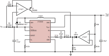
Figure 9. A few components may be used to limit input current for USB and other applications.
Figure 10 shows VOUT dropping when input current reaches 500mA as the load increases. In USB applications where the input voltage is nominally 5V, a Schottky diode is used to limit peak voltages on the SW1 pin.


Figure 10. As load increases, the input current is clamped to 500mA using the circuit of Figure 9.
Conclusion
Analog Devices' new LTC3532 synchronous buck-boost converter simplifies the design of Lithium-Ion or multi-cell powered handheld electronics. With a highly efficient automatic Burst Mode operation, the converter maximizes battery life in portable devices with widely varying load requirements. Soft start, programmable switching frequency and external compensation make the LTC3532 suitable to a wide variety of applications. Two package options, an MS10 leaded package and a 3mm × 3mm DFN, plus the ability to operate efficiently at high frequency, enable the designer to minimize board area and component height.
关于作者
关联至此文章
产品分类


