概览
设计资源
设计与集成文件
- Schematic
- Bill of Materials
- Assembly Files
- Gerber Files
- Allegro Layout File
- LTspice Simulation File
评估硬件
产品型号带"Z"表示符合RoHS标准。评估此电路需要下列选中的电路板
- EVAL-CN0581-EBZ ($58.35) Configurable USB-C Power Sink Solution
优势和特点
- Selectable Voltage Ranges of 5V, 9V, 12V, 15V, and 20V
- Selectable Current Setting up to 3A (or up to 5A at 20V)
- USB-C 1.3 Compatible
- PD 3.0 Negotiation and Messaging
- Surge Stopper with Reverse Protection and Fault Detection
参考资料
-
EVAL-CN0581-EBZ User Guide (GitHub)2026/4/16
-
CN0581: Configurable USB-C Power Sink Solution (Rev. 0)2023/11/7PDF562 K
电路功能与优势
USB-C is an industry standard 24-pin connector system for transmitting data and power over a single cable. In addition to supporting the fastest data rates of USB SuperSpeed (10 Gbps), USB-C (Rev 2.0) supports bidirectional power delivery at several voltages, at power levels up to 100 W. A negotiation process between the power source and sink determines what level the power source provides. The widespread adoption and corresponding low cost of cables, connectors, power supplies, and chargers make USB-C an attractive alternative to dedicated DC power connectors eliminating many proprietary power adapters for a wide range of applications, even when no data connectivity is required.
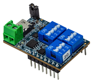
The circuit shown in Figure 1 is a standalone USB-C power delivery (PD) module that adds USB-C power sink capability to projects and devices, replacing traditional power jacks. Voltages of 5 V, 9 V, 15 V, or 20 V at currents from 0.5 A to 5 A are supported, selected via dual in-line (DIP) switches. A hot-swap surge stopper with ideal diode allows charging of large bulk bypass capacitors, and an enable output enables the downstream load after ramp up is complete, while preventing reverse current during faults. No software control is required for operation; the preloaded firmware configuration reads the DIP switches and sets the power delivery object (PDO) voltage and current modes accordingly. Custom configurations can be optionally programmed via an I2C interface.
电路描述
USB-C OVERVIEW
USB-C supports high data rates and increased power delivery between electronic devices. It can transfer data as fast as 10 Gbps, while delivering up to 3 A with 5 V (15 W) over standard cables using the basic configuration channel (CC) detection. The USB-C PD 3.0 specification extends operation up to 5 A and 20 V (100 W). By default, a standard USB-C power source provides 5 V at 3 A, although some noncompliant sources may have lower current capability.
The USB-C specification requires a device to negotiate to be either a power provider (source) or power user (sink) before power transfer takes place. The sink can request a higher voltage and inform the source of its current requirements through the PD negotiation process. If the source can meet the sink's requirements, the source's output voltage is set accordingly. These power levels satisfy the requirement of many portable electronic devices, hence the increasing adoption of USB Type-C for charging and general power delivery. The CN0581 allows the user to set the minimum and maximum bus voltage (VBUS), along with the maximum required operating current using the on-board DIP switches. The following PDOs are supported on the CN0581:
- 5 V, 9 V, 12 V, 15 V — up to 3 A
- 20 V — up to 5 A
Cables, Connectors, and Power Sources
The plugs at both ends of a Type-C cable are identical, allowing for reversible plug-in. Each connector is also reversible, which allows it to be plugged in without worrying about polarity. USB-C cables vary in quality and current carrying capability, a standard cable can typically accommodate bus power up to 60 W at 3 A. In order to achieve 100 W at 5 A, an electronically marked or active cable is required, so be sure that the cable being used is rated for the load current being negotiated. Figure 2 shows the CN0581 plug and receptacle pin configurations.

The USB power source specifications must be interpreted before use in a given application. Not all power sources provide an intuitive combination of voltages and currents. For example, a high-power laptop charger may provide 20 V at 6.5 A (above the official USB-C standard), 5 V at only 1 A (below the standard), and no support for 9 V or 12 V, as compared to a general-purpose 45 W adapter which may provide 5 V, 9 V, 12 V, and 15 V at 3 A (adheres to the USB-C standard) and 20 V at 2.25 A (below the standard). So it is important to validate the USB-C power sources capabilities when connecting a USB-C sink device negotiating for a particular power level.
USB TYPE-C CC DETECTION AND PD MESSAGING
The core of the CN0581 is the MAX77958 standalone USB Type-C and USB power delivery controller.
This device detects connected sources or sinks by first using USB Type-C CC detection, followed by power delivery protocol using USB PD messaging. The MAX77958 protects against overvoltage and overcurrent, detects moisture, and prevents corrosion on the USB Type-C connector. It is compliant with USB Type-C Version 1.3 and PD 3.0, but also has a D+/D- USB switch and battery charging (BC) 1.2 detection to support legacy USB standards.
The CC detection process detects cable presence, orientation, as well as power role and current requirements for the initial 5 V supply voltage. CC detection is new to USB version 1.3 when compared to the legacy USB-C standard in which 5 V is available without any detection. Cable detection occurs when one of the two CC lines is pulled up or pulled down; a device configured as a sink has the CC lines pulled down, whereas a device configured as a source has the CC lines pulled up. The voltage level detected on the CC1 and CC2 lines determines the cable orientation, as well as the source current capability. Table 1 shows the different CC detection configurations. After CC detection, the PD negotiation process continues. If there are multiple valid PDO combinations, the highest power source PDO is requested.
| USB-C Connector | Device Type | Cable Orientation | Source Current Capability |
| USB-C Plug | CC = Logic High (Source) CC = Logic Low (Sink) |
N/A |
CC_voltage < 0.15 V: No connection |
|
USB-C Receptacle |
N/A | CC1 = Logic Low (not flipped) CC2 = Logic Low (flipped) |
Another feature of USB-C is cold-plugging, namely the VBUS voltage is provided only after successful end-to-end detection is completed. This feature makes CC detection mandatory in USBC applications, and the MAX77958 transparently handles all coldplugging and CC operations.
The CN0581 uses the MAX77958 in sink mode to determine the capabilities of the connected source device and optimize power into the surge stopper/ideal diode circuit, as shown in Figure 3.

The MAX77958 has an I2C controller interface that can be pre-programmed with custom firmware to read and write to other devices in the system autonomously without assistance from the application processor. The interrupt output pin can report USB-C PD events and status changes. For systems controlled by an application processor, the device also has with a separate I2C peripheral interface through which the system can read/write and configure internal registers. The MAX77958 has nine configurable GPIOs that can be used for detection, as interrupts, as the enable/disable pin for external devices, or as ADC inputs.
PDO Selection
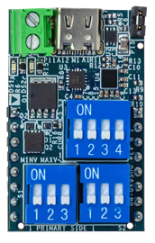
The PDO minimum voltage, maximum voltage, and current requirement are set through DIP switches (Table 2 and Table 3, respectively). Each DIP switch has an open solder blob jumper in parallel such that the board may be configured permanently.
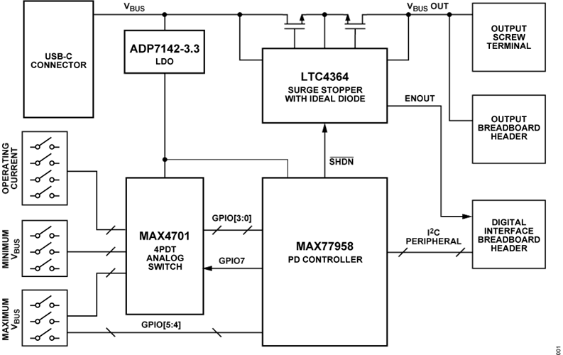
Ten switches are required to select all modes, but the MAX77958 has only seven GPIOs remaining for this function. A MAX4701 dual double pole/double throw (DPDT) switch is used to multiplex the DIP switch signals, as shown in Figure 4. The custom firmware programmed into the CN0581 sequences through all switches and sets the PDO modes accordingly.

| Min/Max VBUS | SW1 | SW2 | SW3 |
| 5V | OFF | OFF | OFF |
| 9V | OFF | OFF | ON |
| 12V | OFF | ON | OFF |
| 15V | OFF | ON | ON |
| 20V | ON | X | X |
| Operating Current | SW1 | SW2 | SW3 | SW4 |
| 0.5 A | OFF | OFF | OFF | OFF |
| 1 A | OFF | OFF | OFF | ON |
| 1.5 A | OFF | OFF | ON | OFF |
| 2 A | OFF | OFF | ON | OFF |
| 2.5 A | OFF | ON | OFF | OFF |
| 3 A | OFF | ON | OFF | ON |
| 3.5 A | OFF | ON | ON | OFF |
| 5 A | OFF | ON | ON | ON |
| 4.5 A | ON | OFF | OFF | OFF |
| 5 A | All Other Combinations | |||
The multiplexing switch can be configured in several different configurations for 5 A operating current. For a complete list, visit the CN0581 User Guide.
SURGE STOPPER WITH IDEAL DIODE
With USB Type-C comes new challenges in system protection. While PD negotiation and the single, standardized, reversible connector mitigate several mechanical and cable fault conditions, an LTC4364-2 hot-swap and ideal diode controller provides protection from high power fault conditions, along with robust power-up into large bulk bypass capacitors.
The surge stopper section of the circuit consisting of Q1, driven by the LTC4364-2's HGATE control pin, provides several functions. It qualifies the input voltage, only turning on when the input voltage is between 3.5 V and 21.8 V. Once this condition is met, the HGATE current source is enabled, ramping the output voltage into up to 1000 μF of bulk bypass capacitance.
Q2, driven by the LTC4364-2's DGATE pin, functions as an ideal diode, preventing reverse current flow in the event the output voltage rises above the USB-C source's voltage due to a fault condition in the power sink circuit, as may occur if the circuit can accept power from multiple sources. Figure 5 shows the surge stopper designed around LTC4364-2 surge stopper with ideal diode control.

Overcurrent Fault
The LTC4364-2 features an adjustable current limit that protects against excessive load current and short circuits. During an overcurrent event, the HGATE pin of LTC4364 is reduced to limit the voltage across the 7 mΩ sense resistor between the SENSE and OUT pins to 50 mV, corresponding to 7.1 A nominal. Upon entering current limit, a current begins charging the 22 nF TMR capacitor according to Equation 1:

where:
ITMR is the TMR pin current.
USB_VBUS_RAW is the voltage input from the USB-C source.
VBUS_OUT is the voltage output from the LTC4364-2.
The timer expires when the capacitor voltage reaches 1.35 V, after which HGATE is pulled low, turning Q1 off. This corresponds to a time of approximately 3 ms when first entering current limit, dropping to 400 μs if a 20 V VBUS_OUT is short-circuited. After the overcurrent fault condition has been removed and a cool down period has transpired, the HGATE pin is allowed to pull back up and turn on Q1.
Input Overvoltage Fault
At power-up, if the LTC4364-2 OV pin voltage is higher than its 1.25 V threshold before the 100 μs internal power-on-reset expires, or before the input undervoltage condition is cleared at the LTC4354-2 UV pin, the HGATE pin will be held low until the OV pin voltage drops below its threshold. The nominal value set for the CN0581 input overvoltage fault is 21.8 V.
Input Undervoltage Fault
When the voltage at the LTC4364-2 UV pin is below its 1.25 V threshold, the surge stopper is off. Once the UV pin voltage rises above the UV threshold plus the UV hysteresis (50 mV nominal), the HGATE pin is allowed to pull up without going through a timer cycle. The nominal value set for the CN0581 input undervoltage fault is 3.5 V.
Output Overvoltage Fault
The LTC4364-2 limits the voltage at the OUT pin during an output overvoltage fault. If the voltage at VBUS_OUT is higher than 24.5 V, set by the FB pin resistors; for longer than the timeout period set by the timer capacitor, an output overvoltage fault is detected, and the surge stopper turns off. After the output overvoltage fault condition has been removed and a cool down period has transpired, the surge stopper of LTC4364-2 turns on again.
POWER ARCHITECTURE
Figure 6 shows the complete power architecture of the CN0581. An ADP7142 provides a regulated 3.3 V for the system I/O voltage (VIO), which sets the GPIO and I2C bus logic levels.

The total power loss measured on the board at 20 V with a 5 A load is less than 1 W, and the voltage drop across the ideal diode is about 0.16 Ω at the same load of 5 A.
常见变化
For applications with a fixed set of PDO configurations, the MAX77958 firmware can be customized and the switches can be removed if the number of configurations can be handled on the MAX77958 GPIO pins directly. See the MAX77958 Customization Script and OPCode Command Guide for more information.
The CN0581 has the LTC4364-2 input OV/UV thresholds, current limit, and hot-swap ramp rate set to accommodate the entire 5 V to 20 V range at maximum current, and a maximum capacitance of 1000 μF. All of these parameters can be adjusted by changing the appropriate configuration components, refer to the LTC4364-2 data sheet.
In applications in which the power adapter and application circuit are well-matched, the LTC4364-2 can be eliminated entirely. If the circuit has an enable input, the VBUS_OUT_EN control signal can be used to hold the circuit off until VBUS is stabilized.
To interface ENOUT pin to a microcontroller, a comparator such as the ADCMP350/ADCMP354/ADCMP356 can be used to obtain a logic level from 2.25 V to 5.5 V with any input from 0 V to 22 V.
电路评估与测试
This section outlines the general setup and circuit evaluation procedure for CN0581. For complete step by step instructions, refer to the CN0581 User Guide.
EQUIPMENT NEEDED
- EVAL-CN0581-EBZ
- USB-C power source capable of delivering 100 W
- USB Type-C cable (rated for 20 V and 5 A)
- DC2132A Constant Voltage, Constant Current Bench Supply (used as a typical example load)
- 8.5 Ω, 20 W power resistor
- Additional 220 μF capacitor (for emphasizing ramp-up current)
- Voltmeter or multimeter
- 4-channel scope
- Current probe
GETTING STARTED
- Configure the EVAL-CN0581-EBZ:
- Connect the CN0581 jumper to select the 3.3 V logic voltage.
- Set the CN0581 PDO minimum and maximum bus voltage to 15 V.
- Set the CN0581 PDO maximum current to 3 A.
- Connect the 220 μF capacitor at the output of CN0581, observing polarity.
- Connect the EVAL-CN0581-EBZ output to the DC2132A input terminals.
- Set the DC2132A output to 12 V.
- Add an 8.5 Ω resistor to the output of DC2132A.
- Connect the ENOUT pin from the EVAL-CN0581-EBZ to the EN/UV pin of the DC2132A's buck converter.
- Connect the EVAL-CN0581-EBZ to the USB-C source via the USB cable.
- The complete setup should look like the block diagram shown in Figure 7.

TEST RESULTS
Figure 8 and Figure 9 show the results of the voltage ramp-up, PD negotiation process, current during ramp-up and operation, and the enable signals. Upon connection of the USB-C power source, the following events occur:
- USB_VBUS_RAW rises to 5 V, the default output of the source.
- The CN0581 negotiates with the source (in this case 15 V/ 3 A PDO), and USB_VBUS_RAW output rises to 15 V.
- The MAX77958 drives the VBUS_OUT_EN signal high, enabling the LTC4364-2.
- The LTC4364-2 HGATE charge pump turns on, ramping the output voltage up. During this time, the current into the 220 μF bulk capacitance is a constant 600 mA.
- Once the hot swap MOSFET is fully enhanced, the LTC4364-2 ENOUT signal goes high-impedance, enabling the DC2132A.
- The DC2132A output rises to 12 V and the load resistor draws 1.4 A, corresponding to 1.2 A from VBUS_OUT.


