AN-2582: Design Considerations of High VOUT Step-Down DC/DC Switching Regulators
Abstract
With high efficiency and high density, DC/DC step-down switching regulators for high VOUT applications have been receiving increasing popularity as systems become more complicated and power hungry. This application note introduces some practical design considerations and challenges of step-down switching regulators with high VOUT, such as how to maintain the normal operation of the bootstrap circuit. The practical considerations are presented together with the guidelines to support the smooth operation of the switching regulator even under some challenging corner cases.
Introduction
Step-down DC/DC switching regulators are widely used in the power conversion applications. Compared to linear regulators, switching regulators are advantageous in many aspects, including output current capability, efficiency, solution size, etc. These advantages are further amplified as the step-down ratio rises. Monolithic power management ICs with integrated power MOSFETs provide a compact and convenient way of leveraging the step-down DC/DC (buck) switching regulators in a wide range of applications. The corresponding design notes and guidance on monolithic buck ICs are well established and understood.
Buck switching regulators are not only suitable point of load (POL) power supplies, but also play a critical role on the intermediate bus rails. These intermediate bus converters typically require higher voltage level and power as they feed into multiple downstream regulators and loads. Thus, there is a growing trend to adopt as many buck regulators as possible in the system design.
As systems become more complicated with more advanced functions, their power consumption keeps increasing, as well as the power distribution losses. To address this problem, system designers continue elevating the intermediate bus voltage level from 12V to 24V, now even further to 48V. The high VOUT buck regulator design is more challenging as the duty cycle, switching loss, inductor core loss, and power MOSFET stress all increase substantially. The goal of this application note is to summarize key design considerations for a buck switching regulator design with high output voltage.
Bootstrap Circuit Considerations
Buck switching regulators that employ an N-channel top FET require a special power scheme to provide its gate drive voltage, since the source of its top FET sits at SW node, whose voltage level swings up and down between 0V and VIN. A popular method to solve this problem is a simple low-cost bootstrap circuit [1]. Typically, the bootstrap circuit only requires an additional capacitor CBST and a diode. With one terminal connected to the SW node, the bootstrap capacitor CBST can supply the power to drive the top FET and other auxiliary circuits, no matter where the SW voltage goes [1].
Nevertheless, the bootstrap capacitor CBST supported by the bootstrap circuit is far from an ideal power supply, as there are limitations (duty cycle, switching frequency, etc.) to keep it functioning smoothly. It is especially challenging to maintain the CBST voltage in high VOUT applications. This section provides an overview and challenges of the bootstrap circuit under high VOUT applications, followed by some guidelines to prevent the malfunction of the bootstrap circuit.
Overview of Bootstrap Circuit
Figure 1 displays a simplified circuit diagram of a buck switching regulator IC equipped with a bootstrap circuit. CBST is connected in series with the bootstrap diode DBST, and parasitic resistance RBST. The bootstrap diode DBST is sometimes implemented with a FET for lower impedance. The other terminal of CBST is often named BST pin. Hence, the voltage of the BST pin is typically higher than the SW node voltage by design. CBST can be either integrated 2 inside the package, or it should be added externally between SW pin and BST pin.

Figure 1. Circuit diagram of a bootstrap circuit for a buck switching regulator IC.
One issue is how to ensure CBST always has sufficient voltage to drive the top FET and its auxiliary circuits. In every switching cycle, CBST can be charged when the top FET is OFF and the SW node voltage is low. At low VOUT with a low duty cycle, typically, the off-time of the top FET is long enough to ensure sufficient CBST voltage. When the top FET is turned on, CBST slowly discharges while serving as the effective power supply to drive the top FET. After charging in the start-up process, the CBST voltage establishes its own steady state to support the normal operation of the top FET and its auxiliary circuits.
Potential Issue of Bootstrap Circuit at High VOUT
However, it is more challenging to charge CBST and ensure the functionality of the bootstrap circuit as VOUT increases; and thus, the part operates at higher duty cycle. The on-time of the bottom FET becomes shorter as VOUT increases, assuming a constant VIN and switching frequency. The time duration available for charging CBST thus keeps shrinking. An extreme case is the dropout condition when VOUT is almost equal to the VIN. Theoretically, the on-time of the bottom FET can drop to zero, ending up with no time to charge CBST. In practice, the on-time of the bottom FET cannot be allowed to drop to zero. There is a minimum off-time requirement for the top FET so that the SW node can be low for a minimum duration to keep the bootstrap circuit alive. However, the minimum off-time requirement (usually <150ns) does not always guarantee sufficiently long duration to charge CBST and satisfactory CBST voltage under all conditions. To improve dropout voltage performance, some regulators skip switch off-times to reduce frequency and increase the effective duty cycle. This makes it even more challenging to keep the CBST charged.
Under high VOUT applications, the light load or no-load condition can further exacerbate the CBST charging situation. When the top FET turns off, the SW voltage can be pulled down very rapidly with the help of considerable inductor current. However, in light load conditions, the low inductor current extends the time it takes for the SW node voltage to go low and start the CBST charging process, effectively reducing the charging time. Especially when the regulator operates under very high duty cycle with minimum off-time, such reduction in CBST charging time can be significant. Higher input voltage, and thus longer SW node fall-time, can further reduce the CBST charging duration.
Moreover, under light load and no-load conditions, the switching regulator often operates under discontinuous conduction mode (DCM) to boost the efficiency. In this case, when the bottom FET is ON, its channel is shut OFF once the inductor current drops below 0A. Then, the SW voltage swings up due to the DCM ringing, hence ending the charging process of CBST. As shown in DCM waveforms in Figure 2 with 55VIN and 43VOUT, both SW voltage (blue waveform) and BST voltage (green waveform) start to oscillate and increase dramatically once the inductor current drops to 0A. The bootstrap diode becomes reverse-biased, and CBST cannot be charged any more until SW is pulled low during the next switching cycle. Even if the oscillation is fully damped, the SW voltage stays at the level of VOUT and still disables the CBST charging path.
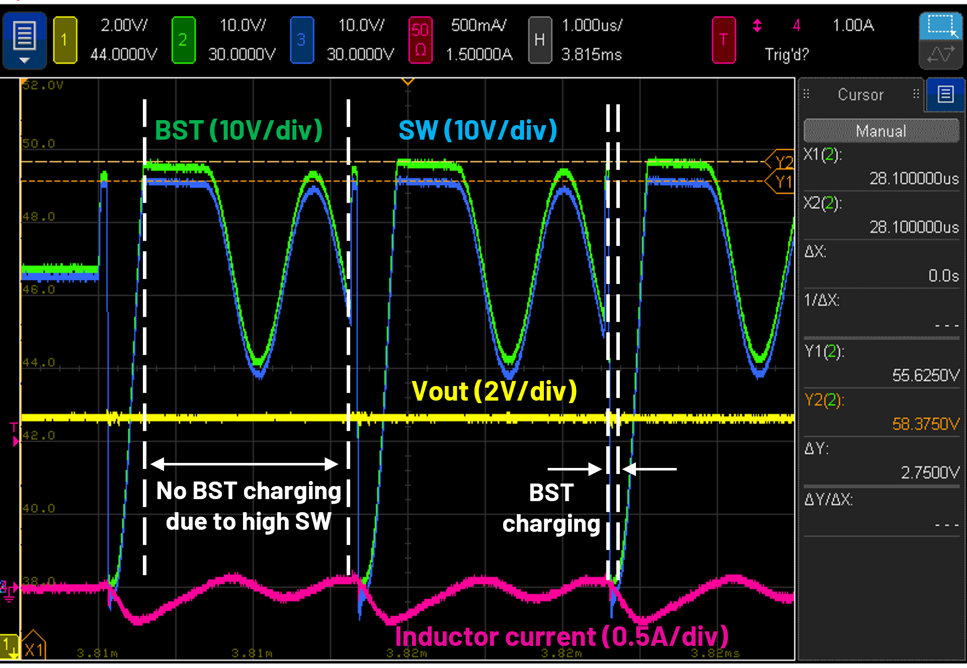
Figure 2. DCM operation of a buck switching regulator IC (under pulse-skipping mode) at 55VIN, 43 VOUT, 2mA load.
Hence, the focus should be the time interval before the inductor current reaches 0A under DCM. This interval is the effective charging time of CBST, called 3 𝑡𝐵𝑆𝑇,𝐷𝐶𝑀 in this application note. Since the peak inductor current is quite low under light load/no-load conditions, it takes a very short period for the inductor current to turn negative. 𝑡𝐵𝑆𝑇,𝐷𝐶𝑀 is very short and can be calculated as following.

In the equation, Ipk is the peak inductor current under DCM operation. Lower Ipk results in shorter 𝑡𝐵𝑆𝑇,𝐷𝐶𝑀 to charge CBST. In many DCM cases, Ipk drops as the load current decreases, and it can be calculated as following, as well as 𝑡𝐵𝑆𝑇,𝐷𝐶𝑀.


RL in equations (2) and (3) is the load resistance. In DCM cases under the burst mode and some pulse frequency modulation (PFM) modes, Ipk is maintained at a constant level on purpose, no matter how low the load current goes. Hence, these modes can benefit the CBST charge replenishment under the light load and no-load conditions.
In DCM, higher VOUT can further jeopardize the normal operation of the bootstrap circuit. The CBST charging time under DCM is a strong function of the output voltage and the inductance. In all DCM cases (equations (1) and (3)), 𝑡𝐵𝑆𝑇,𝐷𝐶𝑀 is shorter as VOUT becomes higher. Selecting a higher inductance at higher VOUT can prolong 𝑡𝐵𝑆𝑇,𝐷𝐶𝑀. Yet, the selected inductance is often too small for high VOUT applications, which is explained and addressed in the next section of this application note.
With insufficient CBST voltage, the operation of the buck switching regulator is heavily impacted. Each time the top FET turns on, the CBST voltage is checked to ensure it can drive the top FET properly. If the CBST voltage is too low, the undervoltage lockout (UVLO) function is triggered to turn off the top FET and force the bottom FET to conduct current and continue charging CBST. As a result, the duty cycle varies significantly if there is a CBST charging issue, leading to significant VOUT oscillation. Figure 3 displays an example of the resulting output voltage oscillation because of the CBST charging issue. Under the dropout condition at a high VOUT of 40V, the switching regulator has trouble maintaining the CBST voltage at light load. The switching regulator must activate the UVLO function of the top FET gate driVINg circuit to force the bottom FET to pull down the SW voltage and charge the bootstrap capacitor. Hence, the bottom FET conduction time is sometimes much longer than its normal on-time in Figure 3. As a result, the inductor current ramps down to −2A rapidly during those abnormal intervals. With only 2mA load, the inductor current oscillates with ~3.8A peak-to-peak ripple, leading to significant VOUT oscillation.

Figure 3. Dropout operation of a Buck switching regulator IC at 40VIN, 40VOUT, 2mA load.
In case the circuits run into the above-mentioned corner cases, here are several design guidelines to support the smooth operation of the bootstrap circuit under high VOUT and high duty cycle conditions.
Design Guideline #1
An external BST diode with low impedance can be installed to charge CBST more efficiently. Adding the external BST diode in parallel with the internal BST diode or FET can help the switching regulator make better use of the limited time window and deliver more charge to the bootstrap capacitor. As long as the SW voltage is low enough, the external BST diode can contribute to a low-impedance path for replenishing the charge stored in CBST.
A Schottky diode with low forward voltage drop and impedance can benefit the CBST charging loop significantly. When the CBST charging process is not active, the external BST diode must endure a reverse voltage same as the internal BST diode or FET, which is approximately VIN. Another critical requirement is low leakage current when selecting the external BST diode. The reverse leakage current must be sourced from CBST while the BST diode is OFF. Hence, a large leakage current can sabotage the benefit brought by the low impedance of the external BST diode. Ensure that the selected BST diode has low leakage current, even at high temperature.
Design Guideline #2
Maintaining a minimum load is another possible solution to support the bootstrap circuit under challenging conditions. This guideline focuses on extending the CBST charging time under light load conditions. In many cases, a minimum load increases the peak inductor current Ipk and prolongs the CBST charging time. The SW voltage can drop more quickly to start the CBST charging process earlier than the condition with a lower Ipk. Moreover, a higher Ipk significantly benefits the CBST charging time under DCM, as shown in equation (1). Generally higher VOUT requires a higher minimum load to achieve long enough CBST charging time.
In summary, the two design guidelines not only leverage the limited CBST charging time more efficiently, but also extend the CBST charging time, especially at no-load and light-load cases. Both design guidelines can be implemented simultaneously under high VOUT and high duty cycle applications.
Inductor Selection for High VOUT Applications
The inductor is one of the indispensable components of a buck switching regulator. The inductor selection is very critical when designing a step-down switching regulator for high VOUT applications. As discussed in the previous section, a special consideration is CBST charging when selecting the inductance for high VOUT applications with high duty cycle.
The inductor is often selected by following the rule of thumb that the peak-to-peak inductor current ripple should be controlled at a satisfactory level, usually 30% to 40% of the load current. The peak-to-peak inductor current ripple can be calculated as follows.

All too often, high VOUT applications require duty cycles greater than 50%, which imposes a minimum inductance requirement to solve the potential sub-harmonic oscillation issue in buck switching regulators with peak current mode control. Details can be seen in application note 19.
Equation (4) suggests that a small inductance can be selected for high duty cycle applications. The inductor current ripple does not increase monotonically as VOUT increases. The inductor current ripple ∆𝐼𝐿 reaches the peak when VOUT is equal to VIN/2 (50% duty cycle), and it starts to decrease rapidly once VOUT exceeds VIN/2 (>50% duty cycle). For example, with constant VIN (24V) and load, the selected inductance drops by 42% if VOUT increases from 18V to 21V. In applications that require high output voltage and high output current, a small inductance can be sufficient to maintain the inductor current ripple at 30% to 40% of the load.
While the switching regulator can operate smoothly with small inductance at the rated VOUT with satisfactory inductor current ripple, it may suffer from excessive inductor current ripple during the soft start-up process. With high VOUT and high duty cycle, the inductor ripple can reach more than 2X the designed value as VOUT ramps up from 0V to the target level; that is, the part is switching from low to high duty cycle during start-up. In light load DCM condition, the transitory high inductor current ripple can undershoot to negative value while the top FET is OFF, which leads to current through the top FET body diode during tristate. Inadvertent reverse current through the top FET body diode in high VOUT condition can potentially cause IC failure, which is discussed in the next section.
Higher inductance is beneficial in solVINg the CBST charging issue under light load and no-load conditions. If the part enters DCM, a higher inductance plays a critical role in extending the CBST charging time, whether the peak inductor current Ipk is a constant or not. As indicated in equations (1) and (3), the inductance should increase accordingly as VOUT rises, to maintain the same CBST charging time.
In summary, a higher inductance can benefit the CBST charging process at light load and no-load conditions, including different DCM modes and forced continuous mode. Under high VOUT applications with high duty cycle, a small inductance might be selected based on the ripple current at full load, while a higher inductance is helpful in supporting the start-up process and the operation at light load. Therefore, the inductance selection should consider its impact on CBST charging time at light load, in addition to the current ripple and loss requirements.
Reverse Current Considerations
Reverse Current and Potential Failure
In a buck regulator, VIN is typically higher than VOUT, and current flows from the input to the output load. However, in certain uncommon conditions, reverse current may occur; that is, inadvertent current flowing in the reverse direction from output to input. At low output voltages, there is no risk from this reverse current. However, at higher output voltages (that is, >10V), sufficient reverse current through the top FET’s body diode may cause part failure [2].
Design Considerations
This section explores the design considerations to prevent the potential high VOUT failure of the buck regulator. In most cases, the reverse current can be observed during power-down, when VIN may unintentionally fall below VOUT. In this condition, reverse current can flow through the body diode of the top FET. Under some circumstances, VOUT decreases slower than VIN due to an “unintentional output hold-up circuit” in the system, very large output capacitance, or other factors.
Figure 4 presents a typical failure waveform of a monolithic buck regulator due to the reverse current during the power-down process. To create the failure, the buck regulator IC is equipped with an intentionally large 200µF COUT and does not have any load. In addition, a large pull-down current is applied to VIN to mimic other system loads on the input rail. Therefore, VIN drops quickly while VOUT stays high, and eventually, VIN dips below VOUT during power-down. Negative inductor current is generated and the resulting current flows through the body diode of the top FET. Reverse current increases rapidly, and eventually, causes part failure.

Figure 4. Typical waveform of part failure due to reverse current during the power-down process.
To prevent part failure due to the reverse current at high output voltages, here are two recommended design guidelines for the application circuit.
Design Guideline #1
A Schottky diode can be added between the SW node and VIN to shunt the energy and limit the current flowing through the internal parasitic body diode. To shunt as much reverse current as possible, the external Schottky diode should feature low impedance, and the diode should be placed next to the IC to minimize additional impedance in the shunt loop. When selecting the Schottky diode, designers should pay attention to the low forward voltage drop and voltage rating. Typically, the Schottky diode with lower voltage rating has lower forward voltage drop and impedance. On the other hand, the Schottky diode must withstand the maximum input voltage of the application. In summary, the reverse voltage rating of the external Schottky diode should be determined first, and then a low-impedance Schottky diode can be selected accordingly.
For example, the recommended Schottky diode selections are listed as following for the 65V/8A monolithic buck regulator from Analog Devices (that is, LT8645S, LT8646S). Other diodes can be adopted if they have similar impedance characteristics.
- RB058LAM-60 (rated at 60V)
- PMEG100T100ELPE (rated at 100V)
- RB160MM-90 (rated at 90V)
Design Guideline #2
This guideline focuses on preventing VIN from dropping below VOUT to avoid reverse current altogether. This can be easily achieved by introducing a proper sequencing scheme. Designers can utilize an external EN signal to disable the part with a proper sequencing such that VOUT is discharged before the system powers down the VIN rail.
Another approach can be implemented by introducing an external EN/UVLO resistor divider (R1 and R2 in Figure 5) to disable the part while VIN is safely above VOUT.

Figure 5. Circuit diagram of a monolithic buck regulator IC with design guideline #1 and #2 implemented.
Note that this guideline counts on a load to discharge VOUT and ensure that VOUT does not exceed VIN. Hence, design guideline #2 may be less effective as the load approaches zero. For the most robust solution, designers may implement both design guidelines in their system.
In addition, some monolithic buck regulator IC parts have been designed to safely tolerate high reverse currents, even at high output voltages; some examples include: LT8640A, LT8638S, and LT8648S.
Conclusion
DC/DC step-down switching regulators with high output voltage are becoming increasingly prevalent due to their high efficiency and current, and small solution size. As systems become more complex and power-hungry, these regulators are a great choice for a wide range of applications (industrial, automotive, etc.). However, designing these regulators with high VOUT can be challenging as there are many user cases to consider, such as start-up, power-down, light load, etc. This application note provides comprehensive considerations and guidelines to tackle design challenges under high VOUT. Design considerations and guidelines regarding the bootstrap circuit are covered thoroughly to maintain the bootstrap circuit operation under high VOUT and high duty cycle applications. Inductor selection guidelines under high VOUT are revisited. How to handle the reverse current is also demystified in detail.
参考电路
- Andrea Merello, “AN-1123, Bootstrap Network Analysis: Focusing on the Integrated Bootstrap Functionality.” Infineon Inc.
- Noora Wang, Ryan Hu, and Milo Zhu, “Methods to Eliminate Damage Caused by Reverse Current in Synchronous Buck Converters.” Texas Instruments Inc., May 2019
作者