AN-1516: 利用低失真差分ADC驱动器AD8138和双通道、4.2 MSPS、 14位SAR ADC AD7357实现直流耦合、单端转差分转换
电路功能与优势
图1所示电路可对4.2 MSPS、14位逐次逼近寄存器(SAR)模数转换器(ADC)AD7357的双极性输入信号进行直流耦合、单端转差分转换。该电路能够提供充足的建立时间和低阻抗,从而确保AD7357实现高性能。
电路描述
差分操作要求采用两个幅度相等、相位相差180°且以适当共模电压为中心的信号,同时驱动ADC的 VINx++和VINx−引脚。并非所有应用都会预先调理信号以用于差分操作,因此经常需要执行单端转差分转换。对AD7357进行差分驱动的理想方法是采用AD8138之类的差分放大器。该器件可以用作单端转差分放大器或差分转差分放大器。AD8138还能提供共模电平搬移。图1显示如何将AD8138用作直流耦合应用中的单端转差分放大器。AD8138的正负输出端通过一对串联电阻分别与ADC的相应输入端相连,从而将对ADC开关电容输入的负载影响降至最小。AD8138的这种架构使得输出可以在很宽的频率范围内保持高度平衡,而不需要严格匹配的外部元件。图1中电路的单端转差分增益等于 RF/RG,其中 RF = RF1 = RF2 , RG = RG1 = RG2。

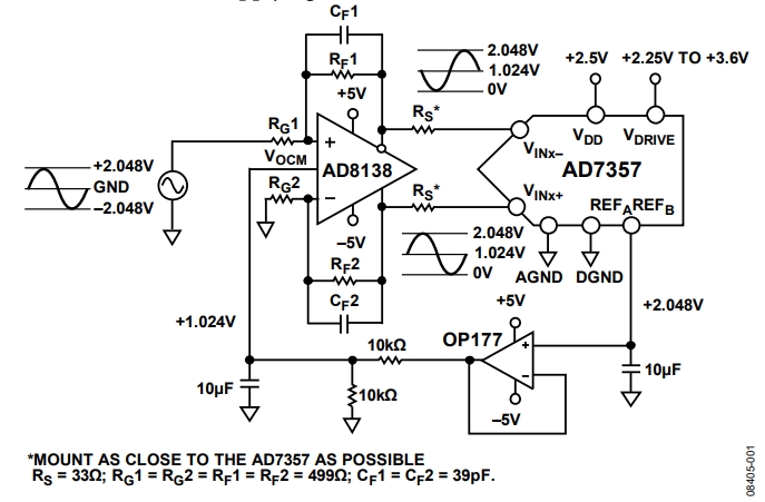
如果所用的模拟输入源具有零阻抗,则所有四个电阻(RG1、RG2、RF1和RF2)相同,如图1所示。如果模拟输入源具有(假设)50 Ω阻抗和50 Ω端接电阻,则RG2值应增大25 Ω以平衡输入端的并联阻抗,从而确保正负模拟输入的增益相同。为了确保阻抗匹配,RF1和RF2也需要略微增大,以补偿因RG1和RG2增大而导致的增益损失。欲了解端接源状态的完整分析,请参考教程MT-076:差分驱动器分析和ADIsimDiffAmp交互式设计工具。
AD7357要求驱动器具有非常快的建立时间,因为若要利用串行接口实现4.2 MSPS吞吐量,采集时间就必须非常短。在转换过程中,AD7357前端的采样保持放大器在第16个SCLK周期的上升沿进入跟踪模式。ADC驱动器必须在采样保持放大器返回保持模式之前建立(对于4.2 MSPS吞吐量、 使用80 MHz SCLK的AD7357,二者相隔39 ns)。AD8138的额定建立时间为16 ns,可满足这一要求。
共模电压由AD8138 VOCM引脚上施加的电压设置。在图1中, VOCM连至1.024 V电压,它由AD7357内部2.048 V基准电压源 通过分压提供。如果要将AD7357的2.048 V片内基准电压源用于系统中的其他地方(如图1所示),则REFA 或REFB的输出必须先经过缓冲。OP177具有高精度性能,是理想的基准电压缓冲器选择。
请注意,在图1中,AD8138采用5 V双电源供电,而AD7357的额定电源电压范围为2.5 V至3.6 V。切记,瞬态或上电情况下决不能超过AD7357的最大输入电压限制(请参考教程MT-036: 运算放大器输出反相和输入过压保护)。
此外,该电路必须构建在具有大面积接地层的多层印刷电路板(PCB)上。为实现理想性能,必须采用适当的布局、接地和去耦技术(请参考教程MT-031:实现数据转换器的接地并解开AGND和DGND的谜团、教程MT-101:去耦技术和 EVAL-AD7357布局)。
常见变化
如需降低成本,可以使用超低失调电压运算放大器OP07D 代替OP177。除输入失调电压(VOS)特性外,二者的性能相似。另外还可以选用AD8628或AD8638,这两款器件具有非常高的精度和非常低的时漂与温漂。
参考文献
ADIDiffAmpCalc John Ardizzoni和Jonathan Pearson,“高速差分ADC驱动器使用规则”,《模拟对话》,2009年5月。
Walt Kester、James Bryant和Mike Byrne,教程MT-031,实现数据转换器的接地并解开AGND和DGND的谜团,ADI公司。
教程MT-036,运算放大器输出反相和输入过压保护, ADI公司。
教程MT-074,精密ADC用差分驱动器,ADI公司。
教程MT-075, 高速ADC用差分驱动器概述, ADI公司。
教程MT-076, 差分驱动器分析, ADI公司。
教程MT-101,去耦技术,ADI公司。