AN-1458: Isolated RS-485 Repeater with Automatic Direction Control
Introduction
TIA/EIA-485, also known as RS-485, is the most widely used balanced transmission standard. Its differential signals and wide common-mode voltage range establish a robust approach for long distance communication. However, when the RS-485 system runs for over 1200 meters, signal attenuation and ground potential differences make the data transmission unreliable. Figure 1 shows a signal and power isolated RS-485 repeater circuit, which addresses the problems of signal attenuation, electrical noise, and ground potential differences on a long cable network. The RS-485 repeater circuit in Figure 1 includes an Analog Devices, Inc., iCoupler® signal and power isolated ADM2587E RS-485 transceiver. The ADM2587E is certified by UL 1577 with a 2.5 kVrms withstand voltage, offering high voltage transient protection for the RS-485 network. The circuit shown in Figure 1 solves the problem of RS485 signal attenuation by boosting the signal at the output of the repeater circuit.

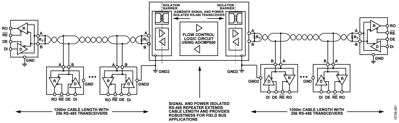
An RS-485 repeater requires flow control, which is essential for controlling the direction of communication on the RS-485 bus. Using the ADCMP600 high speed, complementary metal oxide semiconductor (CMOS) comparator allows high speed flow control and directionality, which results in a reliable communication system. A half-duplex RS-485 network allows data transmission in both directions on only two wires. This application note discusses two ways to implement an automatic direction control RS-485 repeater, as well as the advantages and disadvantages of each method.
Galvanic isolation is ignored for simplicity when describing the flow of operation in the Automatic Direction Control section. Galvanic isolation is both required and essential for operation of the RS-485 repeater circuit shown in Figure 1. Non-isolated RS-485 repeaters are vulnerable to large ground potential differences. It is necessary to isolate at each repeater to reduce the failure risk of the whole system. By using a fully integrated signal and power isolated RS-485 transceiver, the ADM2587E, a simple design of a dual isolated RS-485 repeater is described in this application note.
Typical Application
RS-485 transceivers are designed for operation over long distances, but they can only operate over long distances at low data rates. A low data rate for RS-485 applications is 10 kbps. To operate at higher data rates over longer distances (for example, 50 Mbps over 100 meters), or at lower data rates over much longer distances (for example, 10 kbps over 1200 meters), the isolated RS-485 repeater is an ideal solution for industrial automation networks, including programmable logic controllers (PLCs) and robots.
RS-485 networks are commonly used for communication between the elevator host controller (EHC) and individual elevator control modules (ECMs) in building technologies. With cables in motion, and large motors and inductors in proximity, rugged communication systems are required. The isolated RS-485 repeater provides improved communication reliability in these harsh environments.
For existing installations of solar inverters, which do not include iCoupler isolation robustness on the communications port, the isolated RS-485 repeater is a powerful drop-in solution. The compact, isolated RS-485 repeater delivers robust isolation protection against electrical noise in electromagnetic capability (EMC), harsh solar environments.
For energy metering (E-metering) applications, the isolated RS-485 repeater can be used for reinforced isolation protection at the communications interface, providing user safety protection from the high voltages and currents measured from the single-phase or 3-phase E-metering system.
Automatic Direction Control
Consider a typical, half-duplex RS-485 bus as shown in Figure 1. The 2-wire multipoint network allows data transmission in both directions, but only in one direction at a time. The repeater must be able to sense on which side the signal is coming in and must be able to send it out on the other side. Two physical layer direction control methods are described in the Byte Timing Direction Control section and the Bit Timing Direction Control section; software control, which takes more design effort and can be customized to a certain PLC system, is beyond the scope of this application note. Galvanic isolation is ignored for simplicity when describing the flow of operation in the Byte Timing Direction Control section and the Bit Timing Direction Control section.Byte Timing Direction Control
In byte timing direction control, when data arrives on one side of the repeater, the receiver output (RO) triggers a one-shot pulse, which in turn enables the driver on the other side, as shown in Figure 2. The pulse must sustain long enough to allow the driver to transmit the entire data packet.

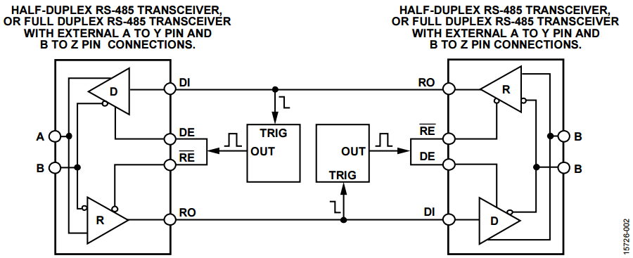
This straightforward solution can be implemented simply by choosing a configurable one-shot pulse generator, such as LTC6993-3 from Analog Devices. In bus idle status, both transceivers are held in receive mode by a fail-safe high condition. When data is present on the RS-485 A and B bus pins, the first corresponding falling edge on the receiver output (RO) pin triggers a one shot pulse. The pulse width must be set in advance by connecting the proper value of resistors to LT6993-3. In this manner, the repeater is not expected to function if the data rate changes during communications. The data rate is fixed for byte timing direction control.
Bit Timing Direction Control
By replacing the one-shot generators with Schmitt triggers, a more flexible direction control is presented in Figure 3. Instead of enabling the driver when the data packet transmits, the Schmitt trigger enables or disables the driver on a bit basis. The bit timing direction control method is independent of the bit speed on the RS-485 bus.

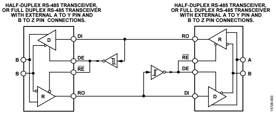
Similar to byte timing direction control, with bit timing direction control, both RS-485 transceivers are held in receive mode when the RS-485 bus is in idle state. On the very first logic low bit when data is present on the RS-485 A and B bus pins on one side of the repeater, the RO changes from high to low and the output of the Schmitt trigger changes from low to high. The ADCMP600 is used as a Schmitt trigger in Figure 3. Subsequently, a logic high bit is present on the RO pin, the rising edge of the high bit switches the trigger output of the ADCMP600 again, and the driver is disabled. A logic high status transmits on the other side of the repeater as the equivalent of bus idle status, which is realized by the RS-485 transceiver fail-safe function. A data rate independent RS-485 repeater design may have interlocking errors, which can happen during low to high data transitions. Because some RS-485 drivers have longer propagation delays than the receiver, an interlocking occurs when both drivers are enabled, which requires a built in delay mechanism to avoid this situation.
Fail-Safe Receiver
The fail-safe function is critical to both direction control methods (see Figure 4), whereas Figure 1 shows a RS-485 network without any fail-safe biasing resistors. Modern RS-485 transceivers have a true fail-safe feature, offering a logic high receiver output feature for bus idle conditions.

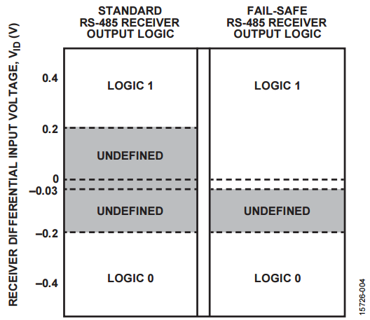
As shown in Figure 4, the standard RS-485 receiver output is undefined when the differential voltage on the bus is within the ±200 mV range. One way to implement a fail-safe high condition is to use biasing resistors, which set the receiver output high as long as they keep the differential bus voltage higher than 200 mV during the bus idle condition. However, the biasing resistors are also common-mode loads to the bus, thereby reducing the bus nodes significantly. On the other hand, the true fail-safe receiver shifts the positive threshold from +200 mV to −30 mV, resulting in the receiver output being high even if the differential voltage on the bus equals zero.
Circuit Implementation
To build a bit timing direction control RS-485 repeater, consider three separate subfunction blocks: the RS-485 transceiver, a Schmitt trigger, and a delay circuit.
RS-485 Transceiver
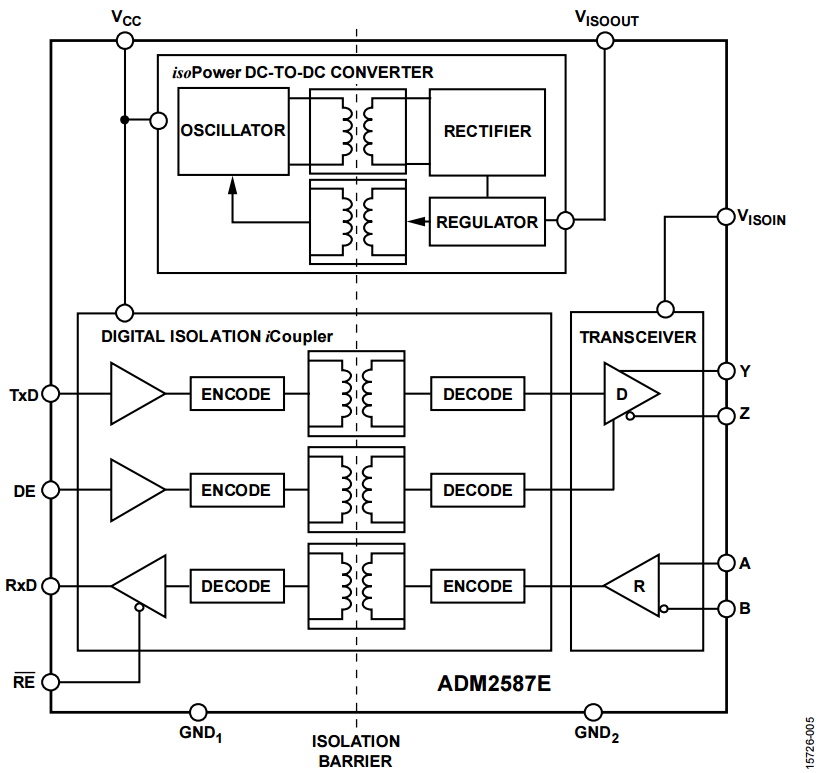
The ADM2587E, shown in Figure 6, is a fully integrated signal and power isolated data transceiver. The RS-485 transceiver includes an integrated, isolated dc-to-dc power supply, which makes it a perfect choice for an isolated RS-485 repeater. Its receiver inputs have open- and short-circuit fail-safe features that ensure the receiver output is high when the inputs are open or shorted. During bus idle conditions, when no driver on the bus is enabled, the voltage across a terminating resistance at the receiver input decays to 0 V and the receiver output is guaranteed to be high. The ADM2587E eliminates the need for an external dc-to-dc isolation block and supports up to 256 nodes on one bus with the true fail-safe function.

Schmitt Trigger
Figure 5 shows an inverting Schmitt trigger in single-supply operation. A Schmitt trigger can be implemented by using a very fast comparator (ADCMP600) and positive feedback networks. The resistor divider (R2 and R1) creates a positive reference voltage that is compared with the input.

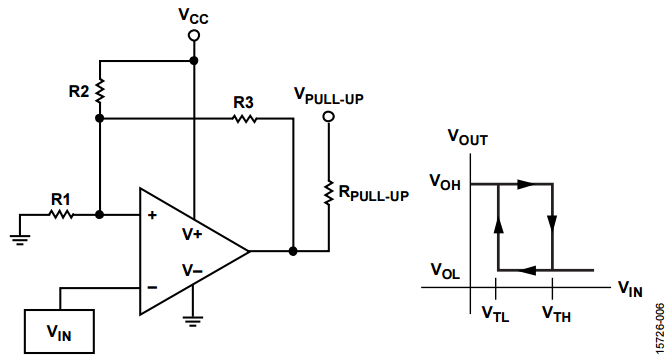
VTL is the low threshold voltage for the receiver outputs—output low voltage (VOL)—output high voltage (VOH)—to change from low to high. VTH is the high threshold voltage for the receiver output to change from high to low.
The hysteresis voltage is essentially the difference between VTH and VTL, which ensures the noise transient does not result in false triggering.
In Figure 1, the RS-485 repeater operates with 5 V single supply (VCC). The hysteresis voltage is set to 1.2 V (VTH = 2.4 V, VTL = 1.2 V). More information on the VOH and VOL voltages can be found in the ADCMP600 data sheet. Under the given conditions, the resistor values can be calculated through the following equations:

Delay Circuit
The maximum propagation delay of the ADM2587E driver is 700 ns while the delay of the receiver is around 90 ns, typically. This timing difference can cause an unwanted logic low on the receiver output (RO). To avoid an unwanted logic low, a low to high delay circuit implements before the Schmitt trigger, as shown in Figure 9.

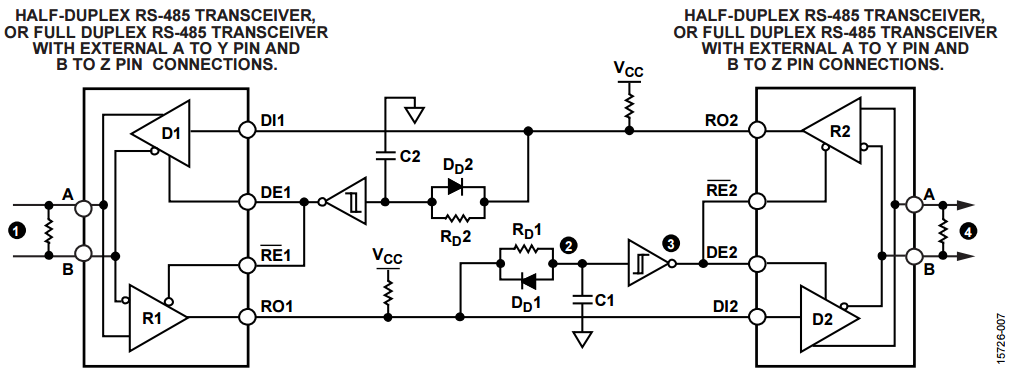
When RO1 becomes high, C1 through RD1 slowly charges from 0 to VTH. Ensure the delay time is longer than the low to high propagation delay, tPLH, of the driver. For a given C1, the value of RD1 can be calculated by the following:

Experiment Result
The ADM2587E bus pins, A, B, Y, and Z, are connected together for half-duplex mode. For half-duplex operation, A connects to Y and B connects to Z. Figure 7 shows test results from the RS-485 repeater discussed throughout this application note. The data rate runs at 40 kbps, Channel 1 represents the differential input signal, and Channel 2 measures the differential output signal. The delay circuit causes the pulse at the rising edge of the output signal, then the differential voltage (VOD) returns to 0 V. For the fail-safe receiver on the bus, the receiver can interpret the pulse and 0 V VOD as logic high; otherwise biasing resistors are required.

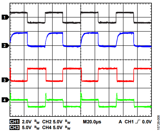
Figure 8 shows the charging slope of the delay circuit, which determines when the Schmitt trigger changes its output from high to low. In an opposite transition status, a fast recover diode discharges C1 rapidly, resulting in no delay. This design is tested to support an up to 500 kbps data rate.

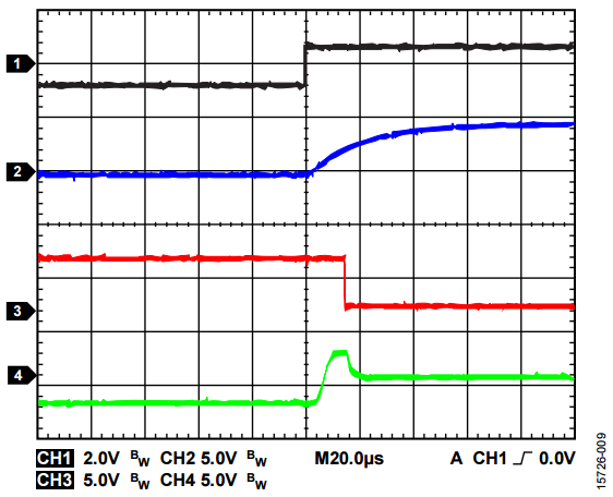
Figure 9 shows a half-duplex bit timing direction control with delay circuit. A full duplex, isolated RS-485 transceiver can also be used with the A pin connected to the Y pin, and the Z pin connected to the B pin, creating a half-duplex external bus connection. The ADM2587E is the recommended RS-485 transceiver.
Figure 9 shows the numbers, 1 through 4, that correspond to the similarly numbered waveforms shown in Figure 7 and Figure 8. For example, in Figure 8, Waveform 3 is the Schmitt trigger output, and Figure 9 shows the corresponding location in the circuit with the number 3 circled in black.
参考电路
Moghimi, Reza. Curing Comparator Instability with Hysteresis, Analog Devices. 2000.
作者

