AN-1141: 用开关调节器为双电源精密ADC供电
简介
与LDO器件相比,开关调节器散发的热量少得多,并且效率更高。因此,开关调节器适合为各类便携设备或无线传感器网络节点供电,从而延长电池续航时间。遗憾的是,开关调节器本身会在输出轨和地处产生纹波和噪声。同时,开关调节器会带来电磁辐射。由于功率开关连续不断的开关操作,这些干扰几乎是不可避免的。受寄生参数的影响,除了开关频率的整数倍处以外,噪声还会出现在意想不到的频率点。

用开关调节器为抗干扰能力很强的电路供电时,虽然存在噪声问题,但如果能有效控制开关调节器的干扰,那么系统性能只会略有下降。
对于典型应用,当数据转换器由开关模式电源(SMPS)供电时,应使目标频段内的总噪声低于噪底,防止它影响转换器。虽然来自开关调节器的带内噪声一般大于噪底,但ADC具有电源抑制能力,噪声在进入信号路径之前会被大幅衰减,因此开关噪声不会降低ADC的性能。
用开关调节器为ADC供电有两个选择:
- 选择低噪声开关调节器,然后利用精心设计的滤波和屏蔽方法消除尽可能多的噪声。
- 估算数据转换器的噪声抑制能力,然后选择具有良好抗扰性能的产品。
实际应用中,两个选择可以同时使用,这样大多数情况下都可以使用开关调节器作为电源解决方案。开关调节器解决方案的优势包括高效率和低温度。
在 CN-0137中,利用双通道输出同步降压开关调节器ADP2114为16位、125 MSPS模数转换器AD9268供电,ADP2114的输出通过一个额外的LC(氧化铁磁珠)滤波器级进行滤波。
与线性电源解决方案相比,测试结果表明,使用DC/DC电源对ADC的性能几乎无影响(见表1)
| 模拟输入频率(MHz) | 线性电源 | DC/DC电源 | ||
| SNR (dBFS) | SFDR (dBc) | SNR (dBFS) | SFDR (dBc) | |
| 10.3 | 79.2 | 92.2 | 79.2 | 92.3 |
| 70.0 | 78.5 | 91.0 | 78.4 | 90.8 |
| 100.3 | 77.8 | 85.8 | 77.7 | 85.6 |
| 140.3 | 76.9 | 85.0 | 76.9 | 84.8 |
| 170.3 | 76.2 | 84.3 | 75.9 | 84.6 |
| 200.3 | 75.0 | 76.9 | 75.0 | 77.0 |
ADP2114的噪声性能通过设计中采用的多项技术来保证,电压纹波典型值小于1 mV。通过额外的滤波,其噪声性能甚至能达到与线性电源相当的水平。
实验结果
在本应用笔记中,利用开关调节器为ADC供电,没有采取任何其它滤波或屏蔽措施,只保留了DC/DC电源正常工作所必需的外部元件。根据上述第二个选择,使用两个对电源不敏感的ADC AD7610和AD7612进行测试。本应用笔记旨在查明SMPS对ADC造成了多大的损害,以及这种损害是否可以接受。
AD7610和AD7612是16位电荷再分配逐次逼近(SAR)型模数转换器,具有真双极性模拟输入范围。模拟输入信号不得超过供电轨0.3 V以上。对于±10 V输入,典型电源电压为±12 V。请参阅AD7610和AD7612数据手册 www.analog.com.
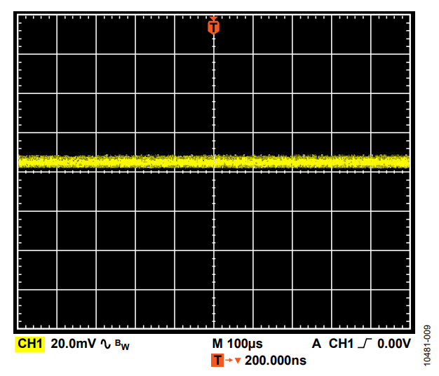
更重要的是,AD7610和AD7612提供出色的电源抑制比。在很宽的频率范围内,它们对AVDD上的电源变化不敏感(见图2)。

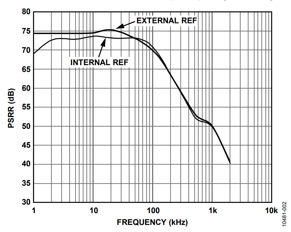
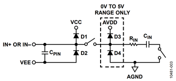
图3给出了AD7610和AD7612输入结构的等效电路。模拟输入首先由高压部分(由VCC和VEE供电)处理,降低到0 V至5 V范围。

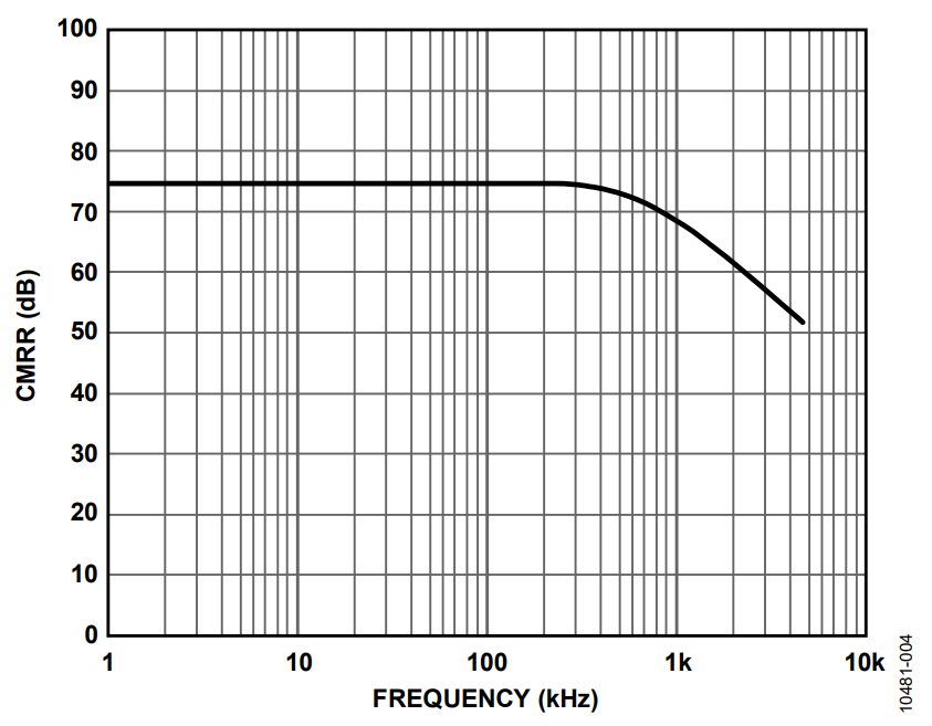
该模拟输入结构支持IN+和IN−之间差分信号的采样。利用此差分输入可以抑制两个输入共有的小信号,如图4所示,它显示了典型共模抑制比(CMRR)与频率的关系。

为给AD7610和AD7612供电,设计了一个使用ADP1613(升压DC/DC转换:5 V至12 V)和ADP2301(反相DC/DC转换:+5 V至−12 V)的5 V至±12 V电源模块。有关ADP2301反相转换器应用的更多信息,请参阅应用笔记AN-1083。
该电源方案可帮助仅有片上5 V电源的客户产生高电流能力、高效率的±12 V电源(见图5)。

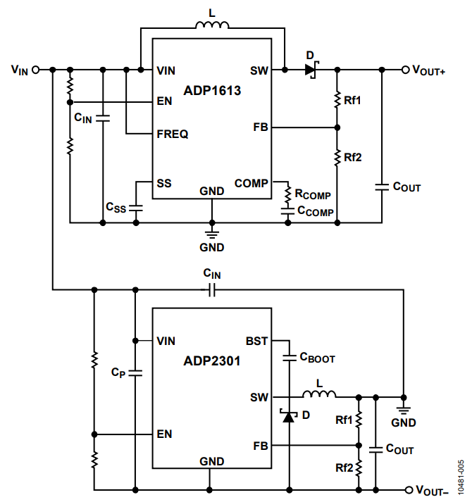
对于SMPS,输出电压纹波可以利用拓扑结构中的一个大电感和输出电容进行抑制。为了应对开关噪声,输出端可以使用一个额外滤波器,这会占用一定的PCB面积。
5 V至±12 V电源模块的基本配置如表2所示。
| 配置 | 输出 | |
| +12 V | −12 V | |
| 开关频率 | 1.3 MHz | 1.4 MHz |
| 输出电感 | 10 µH | 8.2 µH |
| 输入电容 | 10 µF | 10 µF |
| 输出电容 | 10 µF | 44 µF |
| 最大负载 | 400 mA | 200 mA |
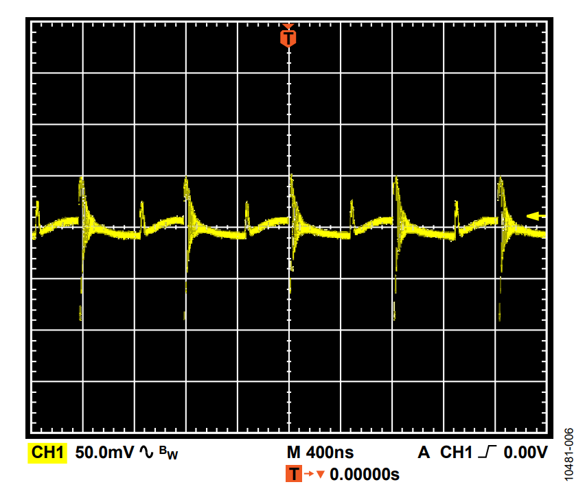
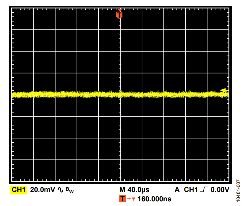
注意,在典型负载(满载的50%)条件下,纹波和噪声性能如下:
-
对于电源模块的+12 V供电轨:
- 纹波 ≈ 20 mV p-p
- 噪声 ≈ 140 mV p-p(示波器为1 MΩ模式)
-
对于电源模块的−12 V供电轨:
- 纹波 ≈ 10 mV p-p
- 噪声 ≈ 50 mV p-p(示波器为1 MΩ模式)


当输出端使用两级滤波器时(第一级是LC滤波器,第二级是磁珠加去耦电容),可以消除大部分纹波和噪声。不过,在本应用笔记提到的所有实验中,使用的都是无额外滤波器的原始输出。
实验1
第一个实验基于AD7612-EVAL和ADuC7026-EVAL执行。ADuC7026-EVAL用于读取转换结果。
AD7612的输入范围配置为±5 V
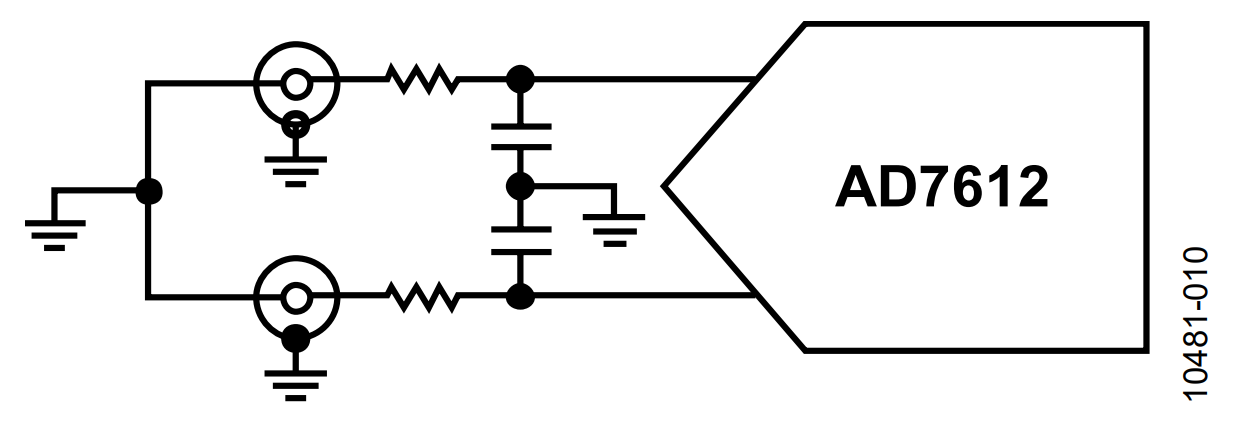
AD7612的模拟输入(IN+和IN−)均直接接地,评估板上的输入缓冲器被旁路(见图10)。

实验中使用了两个电源配置:
- 配置A:AD7612的VCC和VEE由基于ADP1613和ADP2301的±12 V电源模块供电。+5 V AVDD和DVDD由高质量线性直流电源供电。
- 配置B:为进行比较,VCC、VEE、AVDD和DVDD均由高质量线性直流电源提供。
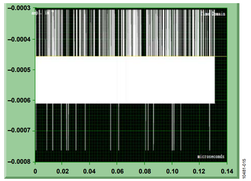
测试过程中执行了16,384次转换。
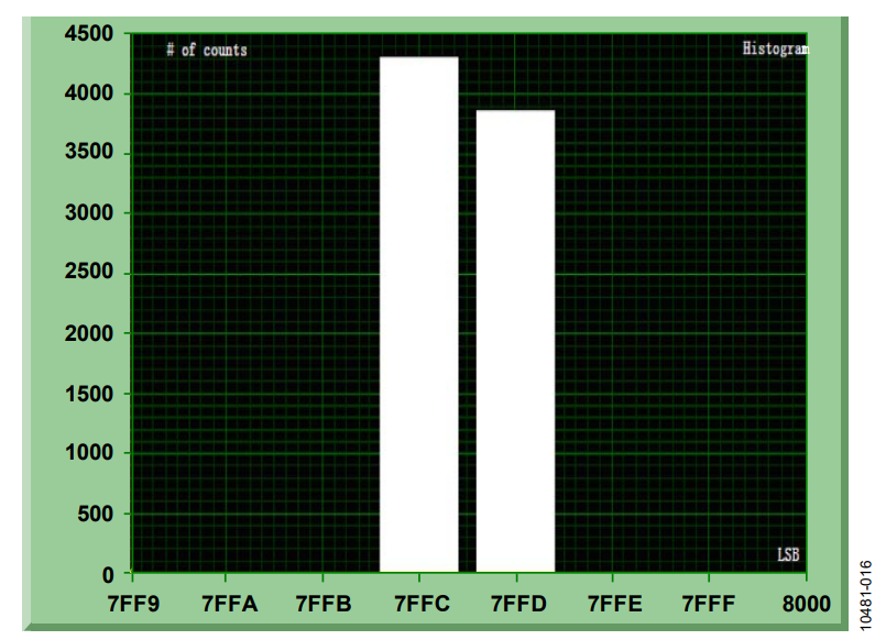
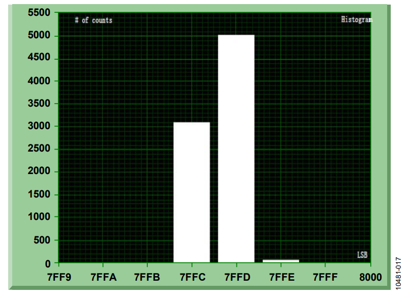
配置A和配置B的测试结果分别如图11和图12所示。

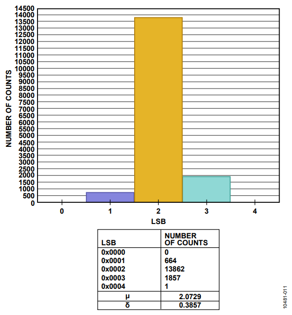

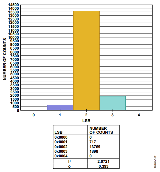
下面是平均值和方差的计算:
对于配置A:
mu (μ) = 2.0729 LSB
sigma (δ) = 0.3857 LSB
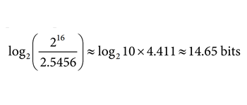
峰峰值噪声 ≈ 2.5456 LSB
峰峰值分辨率 ≈
区间估计:
μ的95%置信区间为[2.0670, 2.0788]
δ的95%置信区间为[0.3816, 0.3900]
对于配置B:
mu (μ) = 2.0721 LSB
sigma (δ) = 0.3930 LSB
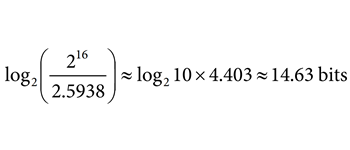
峰峰值噪声 ≈ 2.5938 LSB
峰峰值分辨率 ≈
区间估计:
μ的95%置信区间为[2.0661, 2.0781]
δ的95%置信区间为[0.3888, 0.3973]
峰峰值分辨率的变化在0.03位以内,使用公式SNR = 6.02 N+ 1.76。SNR的变化在0.2 dB以内
实验2
第二个实验基于AD7610-EVAL执行。使用FIFO板(EVAL-Control BRDXZ)和评估软件来分析转换结果。
AD7610的输入范围配置为±5 V。
输入缓冲器使能(AD8021)。AD8021的输入均接地。AD8021为双电源工作模式,采用与AD7610相同的±12 V供电轨(见图13)。

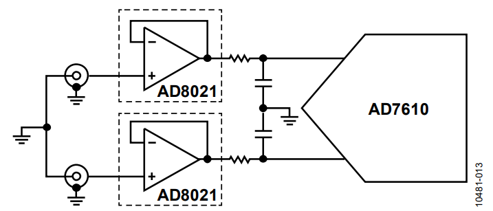
实验中使用了两个电源配置:
- 配置A:利用高质量线性直流电源提供+12 V VCC、−12 V VEE、+5 V AVDD和+5 V DVDD(以及为输入缓冲器供电)。
- 配置B:利用高质量线性直流电源提供+5 V AVDD和+5 V DVDD;利用±12 V SMPS提供+12 V VCC和−12 V VEE(以及为输入缓冲器供电)。
配置A和配置B的测试结果如图14至图19所示。


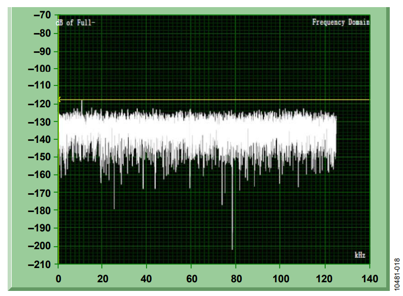

对于配置A:
SNR = 93.40 dB
SINAD = 93.39 dB
对于配置B:
SNR = 93.20 dB
SINAD = 93.18 dB
SMPS对AD7610和AD7612噪声性能的影响非常有限。SNR仅有0.1 dB到0.2 dB的变化,ENOB几乎无变化。如果为SMPS增加额外的滤波器,结果会更好。
AD7610和AD7612数据手册说明了AVDD PSRR的频率响应规格。从实验结果看,VCC和VEE似乎也具有出色的PSRR特性。
滤波考虑
作为二阶滤波器,LC滤波器可在其谐振频率以上提供陡峭的滚降,因而广泛用在DC/DC电源的输出端。然而,开关调节器的性能一般仅在阻性负载下加以规定。如果将一个LC滤波器置于DC/DC电源与阻性负载之间,DC/DC电源就会看到输出端新增一个复负载:
其中,s为拉普拉斯变换的复变量。
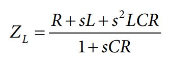

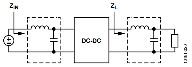
由此看来,作为一个闭环系统,负载条件会影响DC/DC的环路传递函数。闭环系统的带宽和相位裕度会发生变化,这可能引起电路不稳定。附加滤波器对DC/DC电源的影响很复杂。在适当的范围内,带额外LC滤波器的DC/DC电源的瞬态行为与串联RLC谐振电路的阶跃响应类似。
下面是关于LC滤波器选择的半经验原则,可能有助于提高设计的稳定性。
- 一般来说,完全可以将LC滤波器的谐振频率设为高于DC/DC电源的原始环路带宽。
- 如果必须设置较低的谐振频率,可尝试使用较小的电感和较大的电容(较低的Q)。
图21和图22显示了不同LC滤波器的频率响应和瞬态响应的仿真结果。虽然使用了多种电感和电容,但LC谐振电路的谐振频率保持不变。图21和图22给出了负载瞬态变化过程中输出电压的波形:过度波形是在附加LC滤波器之前测得,滞后波形是在附加LC滤波器之后测得。随着电感的提高,负载瞬态过程中发生响铃振荡。

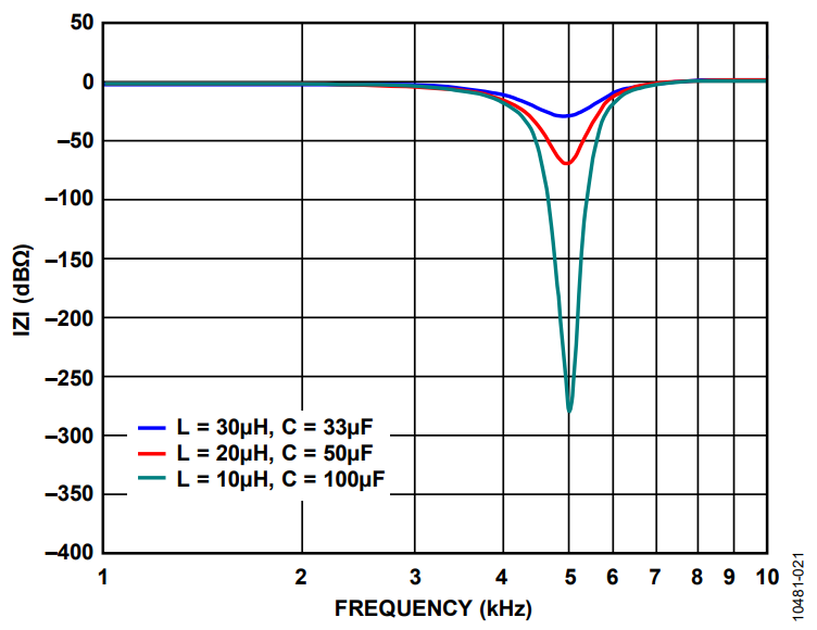

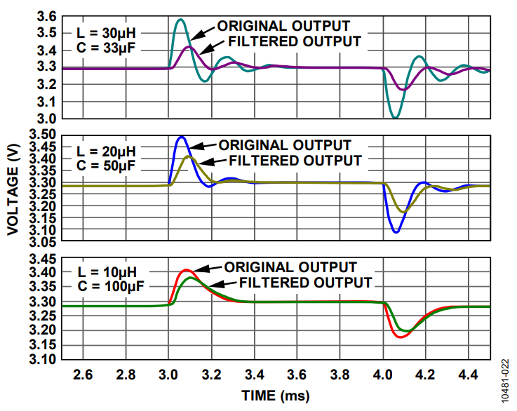
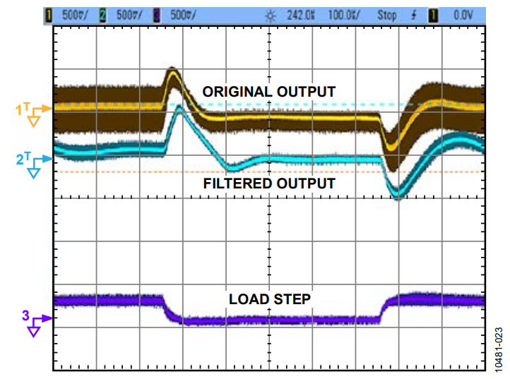
图23所示为ADP1613(12 V输出)的测量结果。输出端增加一个额外LC滤波器(L = 4.7 µH,C = 10 µF)后,噪声大幅降低,而瞬态响应并未有很大变化,系统稳定。

结束语
AD7610和AD7612具有出色的电源抑制性能,其差分输入可确保器件在一定频率范围内具有出色的共模抑制能力。针对此类ADC设计电源时,可以考虑开关调节器。借助外部滤波和屏蔽单元,SMPS的噪声性能可得到进一步改善。对于电源受限的应用,如果要供电的系统具有良好的噪声抑制能力,再加上滤波和屏蔽措施,使用SMPS将能提高能效,而又不会降低系统的性能。
参考文献
AD7610 Data Sheet. Analog Devices, Inc. 2006.
AD7612 Data Sheet. Analog Devices, Inc. 2006.
CN-0137. Powering the AD9268 Dual Channel, 16-bit, 125 MSPS Analog-to-Digital Converter with the ADP2114 Synchronous Step-Down DC-to-DC Regulator for Increased Efficiency. Analog Devices, Inc. 2009.
Kessler, Matthew C. AN-1083 Application Note. Designing an Inverting Buck Boost Using the ADP2300 and ADP2301 Switching Regulators. Analog Devices, Inc.
作者
