Introduction: Measuring Signals
Electronic circuits fall into two broad categories—those that process and transform signals and those that measure signals. Their functions are often combined, as in the IF section of a receiver—which processes the signal (by amplification and demodulation), and also delivers an indication of received signal-strength (the RSSI function), a slowly-varying voltage that may be displayed and/or used for automatic control of variables such as gain and frequency (AGC and AFC).
Circuits that measure RF signal strength, whose fundamental metric is power, are generally called detectors, but only a thermopile (bolometer) measures this quantity directly. Integrated-circuit detectors invariably operate on a voltage sample of the signal to be measured. Circuits of this class are classified by the type of signal transformation they provide. In 1976, Analog Devices supplied the first monolithic "true-rms" detectors for use at moderate frequencies. Now this product line includes devices, such as the AD8361, that have extended this capability to the microwave domain. The accurate determination of signal power, independent of its waveshape (stated otherwise, its probability density function) is important in modern communications systems such as CDMA. Unlike thermal detectors, these true-rms detectors use analog computation to directly implement the relevant equations—at gigahertz frequencies.
Another valuable type of RF detector (also using computation) is the demodulating logarithmic amplifier. As the name suggests, it amplifies the signal, which allows devices of this class to measure small signals, and it demodulates the alternating RF waveform to a slowly-varying "quasi-dc" output. However, unlike the rms detectors, whose output is proportional to the root-mean-squared value of the input voltage, logarithmic detectors deliver an output proportional to the decibel value of the signal level, referenced to a fixed voltage, VINT (defined below). The output, usually a voltage, may be interpreted in terms of either voltage or power, simply by using a different value for a scaling parameter called the "slope".
For RF log amps, it is necessary to use voltage metrics for all the signal and scaling parameters. To define the input level, we will use dBV (here meaning decibels relative to 1 V rms ) rather than refer to "power", in dBm (decibels relative to 1 mW). This is unambiguous, independent of the choice of impedance at the input interface, and appropriate for an IC detector. For example, 0 dBV corresponds to a sine wave of 2.83-V peak-to-peak amplitude; similarly, –60 dBV refers to a 2.83-mV p-p sine wave.
The operation of these RF logarithmic detectors conforms to a function like this:
VOUT = VSLP log(VSIG/VINT) (1)
If base-10 logarithms are chosen [log10(10) = 1 decade], with decibels in mind, the slope voltage, VSLP, can be viewed in terms of "volts-per-decade" in the scaling of the log of the voltage ratio. Since there are 20 decibels in a decade, the corresponding "volts/dB" is just one-twentieth of this voltage. Thus, for a VSLP of 400 mV/decade, the slope can also be expressed as 20 mV/dB. The second scaling parameter, called the "intercept", VINT, is the input voltage at which the log argument is unity. At this voltage, independent of choice of base, the output would be zero, since log(1) = 0. In practice, the finite available gain in an RF log amp, the presence of noise, and other practical limitations result in a value for VINT that is an extrapolated value, typically only a few microvolts, and fixed by the design.
A question then arises as to the precise interpretation of what VINT represents. Is this quantity "volts dc", or perhaps "volts rms"? Or is it some other metric, such as a simple average value, or the peak value? For measurements of ratios from one level to another, the value of VINT is unimportant. However, where it is required to determine the absolute level of VSIG, the measurement accuracy depends directly on the value of VINT in just the same way as a reference voltage in, say, a DVM.
A close study of RF logarithmic amplifiers, which use the technique1 known as "progressive compression", shows another effect not encountered in classical log amp practice, namely, that the effective value of VINT strongly depends on the waveform of the input signal. For that reason, we choose to define VINT for a sinusoidal input, and then provide conversion factors for various other waveforms.
In practice, the control of VINT in an untrimmed production IC cannot be as accurate as is often needed in precision RF metrication. Laser trimming, first used for an RF log-amp in the AD640/641, and more recently in products such as the AD8306, can provide very accurate calibration, using a sine-wave input during calibration. However, while the use of the appropriate conversion factor for a known waveform can maintain good accuracy, there remains the basic problem of waveform-dependence. This poses a problem in contemporary systems where the waveform is both unknown and can vary rapidly.
Measurement of Signal Ratios to 2.5 GHz
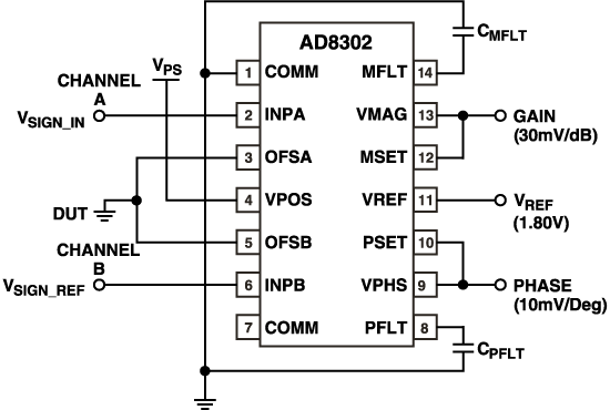
This problem has been addressed, in the AD8302, by the use of two identical log amps integrated in monolithic form, as shown in Figure 1. Each channel is capable of measuring signals over a 60-dB range, from very low frequencies up to 2.5 GHz. The defining function for the amplitude ("gain") output is
VMAG = VSLP log (VA/VB) + VCP (2)
where VA and VB are two independent signals, applied to the two identical input ports of the AD8302, and VCP is the center-point, defined as the value of the output, VMAG, for a level difference of 0 dB. (VSLP and VCP are design choices, made with ease-of-use in mind; both are traceable to a band-gap reference).

The customary fixed intercept, of Equation 1, is eliminated in the AD8302 by taking the difference of the outputs of the two separate log-amps. This key step computes the log of the ratio (VA/VB)*(VINTB/VINTA); and, since the log amps are identical, the second term is very accurately unity, independently of temperature, supply voltage, and numerous production variances.
This elegant elimination of a fixed intercept results in a highly accurate measurement of signal level, in many applications. The primary limitation to the accuracy of the log argument is now the matching of the two co-integrated channels. This novel structure2 opens up many measurement possibilities that would otherwise require the use of two distinct log amps, with their inherent differences in slope and intercept calibration. The AD8302 is the first IC to permit the direct measurement of ac signal ratios. This unique capability for measuring gain/loss and the relative phase (see below) between two signal ports, over a very wide range of frequencies, will be of value in many other applications.
Figure 2 illustrates the output voltage variation as a function of signal ratio (which, for example, may correspond to the gain or loss of a channel being monitored) at frequencies ranging from 900 MHz to 2.2 GHz. The signal level presented to channel B is fixed while that at channel A is varied from –30 dB to +30 dB relative to channel B. The output, VMAG, demonstrates the precise slope, VSLP, of 20 mV/dB and a center-point, VCP, of 900 mV. The very small deviation from an ideal logarithmic law (Figure 2b) demonstrates the value of using co-integrated log amps.
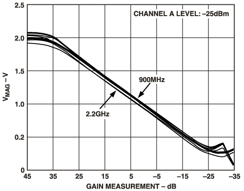
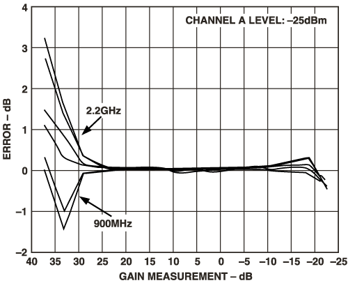
Figure 2. Measurements of signal-level ratios
Measurement of Relative Phase to 2.5 GHz
The AD8302 can also measure the phase difference between two signals, from low frequencies up to 2.5 GHz. Each of the individual log amps generate a "hard-limited" output at its final stage. These signals are applied to the two inputs of a novel multiplier-style phase detector having exact symmetry with regard to its two inputs and a 180° range. The phase output, VPHS, is given by,
VPHS = ±VF (F – 90°) + VCP (3)
where VF is the scaling voltage for the phase output and (F is the phase difference between the two inputs. The choice of sign depends on which two quadrants constitute the 180° phase interval. With the inclusion of this feature, the AD8302 becomes a "network analyzer on a chip".
Figure 3 illustrates phase measurement at 900 MHz, 1.9 GHz, and 2.2 GHz. Here, the phase difference was generated, as a "slip", by slightly offsetting the two input frequencies and allowing the angle to accumulate. The slope of the VPHS output is 10 mV/degree, centered at a VCP of 900 mV. The alternating sign of the slope is apparent as the phase slips through 180° intervals. Figure 3b shows the measurement error. The rapid increase in error near 0° and 180° is due mainly to dead-zones caused by the finite rise- and fall times of the hard-limited signals. The unique ability of the AD8302 to accurately measure phase at these frequencies is a result of the excellent balance of its two tightly- integrated log amps.
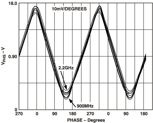
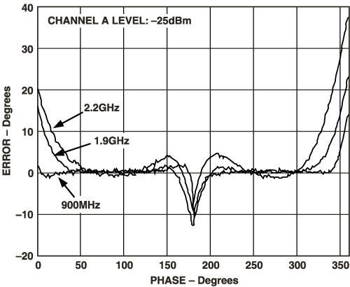
Figure 3. The phase measurement
Using the AD8302
These new capabilities for measuring gain/loss and the relative phase between two signal ports will be of value in many RF and IF applications. The functionality, versatility and compact form-factor of this "network analyzer on a chip" are ideally suited for in-situ diagnostics and monitoring of system parameters and for feedback and feed-forward linearization and control of sub-systems. Here are a few applications of the AD8302.
The measurement of absolute signal level is now possible using a known ac reference. As shown in Figure 4, the reference signal, applied to Channel B, creates an effective intercept of value VB. When the two signals have similar waveforms, the measurement can be very accurate. Even the error due to uncertainty in the slope voltage can be minimized (eliminated, in principle) if one can ensure that the two inputs are close-to-equal in amplitude. This will often be a simple matter to arrange, using an attenuator pad on the larger signal to position the ratio VA/VB close to unity. Centering techniques are valuable when the highest accuracy is needed or where very large dynamic ranges must be handled.
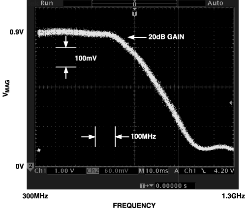
The most useful application of the AD8302 is in monitoring and reporting the gain or loss of a functional block or subsystem. In the example shown in Figure 5, samples of the input and output signals of a 500-MHz IF amplifier with a nominal gain of 20 dB are monitored. By using attenuators and couplers, the two signals are conditioned to be of the same general magnitude. The gain response shows the mid-scale low frequency value, which corresponds to a 20-dB level difference at the amplifier and a 3-dB bandwidth of approximately 500 MHz. The functional block in this example could have been a frequency-translation device, such as a mixer. In that case, the two inputs would be at different frequencies, and the measured quantity would be the conversion gain. Since the waveforms remain similar, that source of error is again eliminated. However, when the input frequencies differ greatly, a systematic offset may occur due to inequalities in the impedance match and the frequency dependence of the scaling of the two log-amps in the gigahertz region.
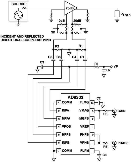
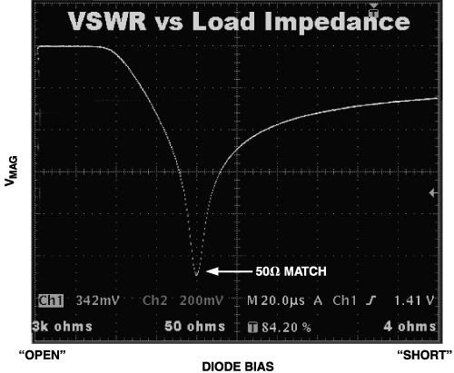
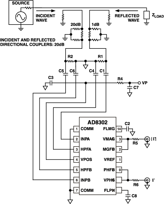
In many communication systems, there is an unpredictable load presented to an external interface port. Variations in this load can lead to changes in system performance, or even to catastrophic failure in extreme cases. It is of great value to provide the means of monitoring the load impedance—or reflection coefficient in RF terms—without perturbing it. In Figure 6, the AD8302 is configured to measure the reflection coefficient of an arbitrary load, which, in this case, is a PIN-diode whose bias is swept to change its impedance. The notch in the response curve represents a near-match to the 50-ohm characteristic line impedance, where the reflected signal is almost zero.
Versatility and Ease of Use
The AD8302 offers several other modes of operation, the result of careful planning and the fundamentally versatile nature of this unusual structure. The previous examples have demonstrated the AD8302 in its typical measurement mode, where the VMAG and VPHS outputs report the signal level and phase difference between its inputs. However, the built-in scaling and center-points of the transfer functions can be adjusted using external resistors and the 1.80-V internal reference provided at the VREF pin.
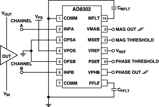
By disconnecting the output pins from the feedback pins, MSET and PSET, a gain- and phase-comparator is realized, as shown in Figure 7. Here, the VMAG and VPHS outputs toggle between 0 V and the maximum output voltage of 1.8 V, depending on whether the signal level and phase difference are greater than or less than the thresholds presented to the MSET and PSET pins.
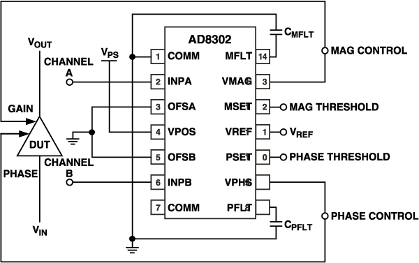
In the controller mode, shown in Figure 8, the VMAG and VPHS pins drive gain/phase-adjusters that are included in the signal chain being monitored so as to servo the overall gain and phase of the system toward the desired set-points presented to the MSET and PSET pins.
The AD8302 has a broad frequency range at its input, ranging from arbitrarily low frequencies (even audio) up to 2.5 GHz. The wide dynamic range of the log amps accommodates not only large changes in relative signal level but also variations in the absolute levels. The output quantities representing the amplitude and phase difference have a maximum small-signal envelope bandwidth of 30 MHz; this can optionally be reduced by adding external filter capacitors.
The AD8302 provides this powerful computational function for the first time in monolithic form using an advanced bipolar process. The excellent log-amp matching, high-frequency capability, and precise scaling of gain and phase measurement, all in a small footprint, open up new opportunities for in-situ monitoring and controlling of RF and IF systems in a non-invasive fashion. Operation from 2.7- to 5.5-V supply voltages is provided at a current of only 20 mA. The product is available in a 14-pin TSSOP package.
参考电路
1 A detailed description of the theory of operation of log-amps can be found in the AD640 data sheet.
2 Patent pending.
致谢
The authors would like to recognize the tireless efforts of Tom Kelly and Shirine Eslamdoust in product engineering, and Ron Simonson and Rick Cory for applications development.


