ADF4030
推荐用于新设计10 通道精密同步器
- 产品模型
- 2
概述
- 10 个 BSYNC 通道
- 精确的 BSYNC 时间对齐 (<5 ps)
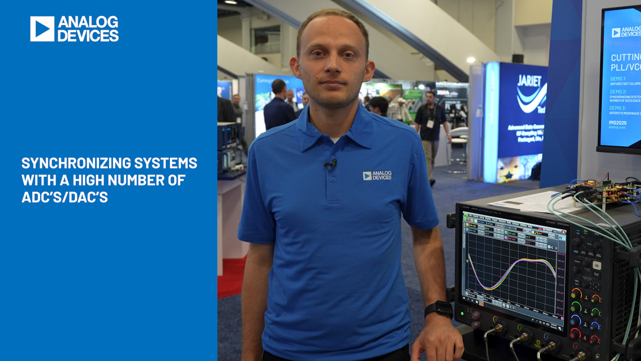
- 实现大型分布式网络中的时钟同步
- 独立可编程的 BSYNC 通道延迟
- 使用双向环回功能对每个 BSYNC 通道进行精确的路径延迟补偿
- 灵活的物理接口支持带直流或交流耦合的 PCB 走线或电缆连接
- 每个 BSYNC 通道支持间断式周期时钟
- 集成式 TDC
- 集成温度传感器
ADF4030 提供 10 个双向同步时钟 (BSYNC) 通道,并接受参考时钟输入 (REFIN) 信号作为频率参考,以在配置为输出的任何 BSYNC 通道上生成输出时钟。ADF4030 的标志性特性是能够将任意一个或多个 BSYNC 通道的时钟边沿相对于选为参考 BSYNC 通道的 BSYNC 通道时间对准至 <5 ps(在设备引脚处)。
ADF4030 非常适合与其他 ADF4030 设备进行多种连接,以同步系统中的时钟信号。每个 BSYNC 都是双向的,允许反转时钟信号的方向来测量传输介质的传播延迟。还支持使用副本路径的往返构造。与使用复制路径相比,往返延迟测量的双向特性大大减少了确定通过 BSYNC 传输介质的传播延迟的误差。该特性使得 ADF4030 能够对多个 ADF4030 器件上的 BSYNC 通道的时钟边沿进行时间对准,而与 ADF4030 系统设计的树状或级联架构无关。双向时钟的优势扩展到 ADF4030 以外的设备(假设这些设备支持双向时钟交换)。
与每个 BYSNC 通道相关的输出分频块都有一个可选的伪随机二进制序列 (PRBS) 生成器,用于 Rev. 0 文档反馈技术支持功能框图图 1。功能框图产生支持 JESD204B 和 JESD204BC 操作的间隔周期时钟信号。
ADF4030 可用作独立差分时间数字转换器 (TDC),以测量到达输入的时钟之间的时间差。
一个 ADF4030 BSYNC 时钟的 RMS 抖动典型值为 4.3 ps。
ADF4030 采用 48 引脚 7 mm ×7 mm,栅格阵列 [LGA] 封装,操作在 −40 °C 至 +105 °C 环境温度范围。
在整个数据表中,字母 x 用于表示任何整数。例如,在 BSYNCx 中,x 指的是从通道 0 到通道 9 的任意通道。
应用
- 5G 时序传输高精度同步
- 相控阵雷达
- 自动测试设备 (ATE) 引脚电子元件
- JESD204B/JESD204C 支持模数转换器 (ADC) 和数模转换器 (DAC) 时钟
参考资料
数据手册 1
技术文章 1
视频 1
器件驱动器 2
ADI 始终高度重视提供符合最高质量和可靠性水平的产品。我们通过将质量和可靠性检查纳入产品和工艺设计的各个范围以及制造过程来实现这一目标。出货产品的“零缺陷”始终是我们的目标。查看我们的质量和可靠性计划和认证以了解更多信息。
| 产品型号 | 引脚/封装图-中文版 | 文档 | CAD 符号,脚注和 3D模型 |
|---|---|---|---|
| ADF4030BCCZ | 48-Terminal Land Grid Array [LGA] | ||
| ADF4030BCCZ-RL7 | 48-Terminal Land Grid Array [LGA] |
这是最新版本的数据手册
软件资源
Evaluation Software 0
找不到您所需的软件或驱动?
硬件生态系统
工具及仿真模型
IBIS 模型 1
LTspice®是一款强大高效的免费仿真软件、原理图采集和波形观测器,为改善模拟电路的仿真提供增强功能和模型。
评估套件


资料
软件


16Tx/16Rx Direct X-Band Sampled Phased-Array/RADAR/SATCOM Development Platform
最新评论
需要发起讨论吗? 没有关于 ADF4030的相关讨论?是否需要发起讨论?
在EngineerZone®上发起讨论