HMC987
LAST TIME BUY3.3V Low Noise 1:9 Fanout Buffer, DC - 8 GHz
- Part Models
- 2
- 1ku List Price
- price unavailable
Overview
- Ultra Low Noise Floor: –166 dBc/Hz @ 2 GHz
- LVPECL, LVDS, CML & CMOS Compatible Inputs
- Up to 8 Differential or 16 Single-Ended LVPECL Outputs
- One Adjustable Power CML/RF Output
- Serial or Parallel Control, Hardware Chip-Enable
- Power-Down Current < 1 uA
- 32 Lead 5mm × 5 mm SMT Package 25 mm2
The HMC987LP5E 1-to-9 fanout buffer is designed for low noise clock distribution. It is intended to generate relatively square wave outputs with rise/fall times < 100 ps. The low skew and jitter outputs of the HMC987LP5E, combined with its fast rise/fall times, leads to controllable low-noise switching of downstream circuits such as mixers, ADCs/DACs or SERDES devices. The noise floor is particularly important in these applications, when the clocknetwork bandwidth is wide enough to allow squarewave switching. Driven at 2 GHz, outputs of the HMC987LP5E have a noise floor of –166 dBc/Hz, corresponding to a jitter density of 0.6 asec/rtHz - or 50 fs over an 8 GHz bandwidth.
The input stage can be driven single-ended or differentially, in a variety of signal formats (CML, LVDS, LVPECL or CMOS), AC or DC coupled. The input stage also features adjustable input impedance. It has 8 LVPECL outputs, and 1 CML output with adjustable swing/power-level in 3 dB steps.
Individual output stages may be enabled or disabled for power-savings when not required using either hardware control pins, or under control of a serial-port interface.
APPLICATIONS
- SONET, Fibre Channel, GigE Clock Distribution
- ADC/DAC Clock Distribution
- Low Skew and Jitter Clock or Data Fanout
- Wireless/Wired Communications
- Level Translation
- High Performance Instrumentation
- Medical Imaging
- Single-Ended to Differential Conversion
Documentation
Data Sheet 1
Technical Articles 1
Quality Documentation 1
ADI has always placed the highest emphasis on delivering products that meet the maximum levels of quality and reliability. We achieve this by incorporating quality and reliability checks in every scope of product and process design, and in the manufacturing process as well. "Zero defects" for shipped products is always our goal. View our quality and reliability program and certifications for more information.
| Part Model | Pin/Package Drawing | Documentation | CAD Symbols, Footprints, and 3D Models |
|---|---|---|---|
| HMC987LP5E | 32-Lead QFN (5mm x 5mm w/ EP) | ||
| HMC987LP5ETR | 32-Lead QFN (5mm x 5mm w/ EP) |
| Part Models | Product Lifecycle | PCN |
|---|---|---|
|
Jul 28, 2022 - 22_0023 Product Discontinuance for Select Analog Devices Parts (ADFXXXX, HMCXXX) |
||
| HMC987LP5E | ||
| HMC987LP5ETR | ||
This is the most up-to-date revision of the Data Sheet.
Software Resources
Can't find the software or driver you need?
Request a Driver/SoftwareHardware Ecosystem
| Parts | Product Life Cycle | Description |
|---|---|---|
| LTC6955 | LAST TIME BUY | Ultralow Jitter, 7.5GHz, 11 Output Fanout Buffer Family |
| HMC7043 | RECOMMENDED FOR NEW DESIGNS |
High Performance, 3.2 GHz, 14-Output Fanout Buffer with JESD204B/JESD204C |
| ADCLK948 | RECOMMENDED FOR NEW DESIGNS | Two Selectable Inputs, 8 LVPECL Outputs SiGe Clock Fanout Buffer |
Tools & Simulations
IBIS Model 1
Evaluation Kits
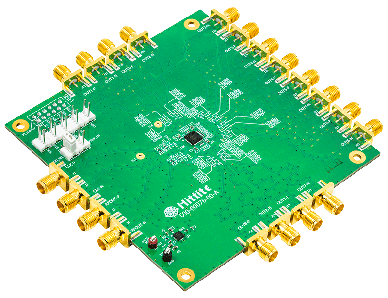
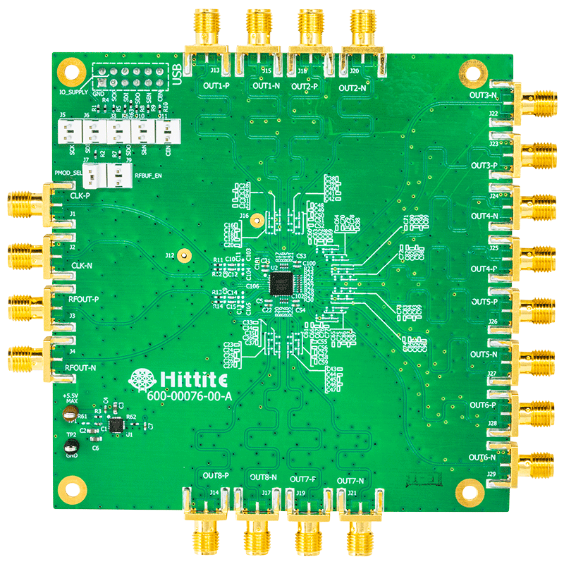
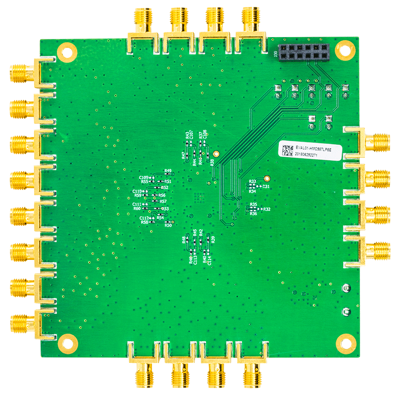
HMC987LP5E Evaluation Board