
RF Front-End Systems for Radar
Analog Devices supplies complete RF front-end solutions for radar applications and phased array antenna. Our large portfolio of power amplifiers in GaN and GaAs technology, low noise amplifiers (mainly in GaAs technology), and switch technology in GaAs, silicon SOI, and GaN technology form Tx/Rx functionality in radar applications. Also available are integrated front ends where all of this functionality resides in one package.
Value and Benefits
- Complete RF Front-End: GaN, GaAs, and SOI tech deliver Tx/R functionality for radar and phased arrays.
- High-Performance Chain: PAs, LNAs, and switches ensure low noise and power efficiency.
- Integrated Beamforming: Single-package T/R modules simplify design and control.
- Reduced Workload: Streamlined deployment accelerates implementation.

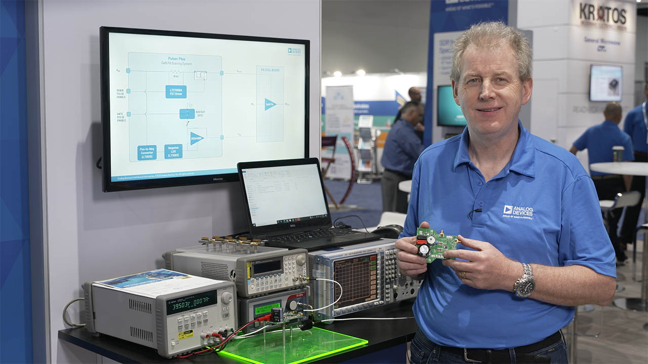
Apollo MxFE: 16Tx / 16Rx X-Band Radar Platform
Watch how four Apollo MxFE™ digitizer ICs on a single board improve multichip synchronization and multichannel calibration methods.

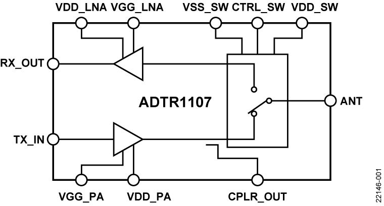
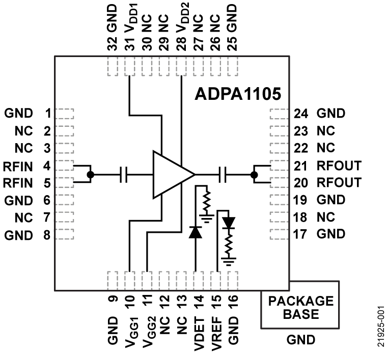
ADTR1107
The ADTR1107 is a compact, 6 GHz to 18 GHz, front-end IC with an integrated power amplifier, low noise amplifier (LNA), and a reflective single-pole, double-throw (SPDT) switch.

Powering Phased Array Radar
High power, high efficiency AESA made possible with ADI’s GaN PAs. Learn about the ADPA1122 20 W GaN power amplifier.
Featured Products
Evaluation Boards


Key Resources


{{modalTitle}}
{{modalDescription}}
{{dropdownTitle}}
- {{defaultSelectedText}} {{#each projectNames}}
- {{name}} {{/each}} {{#if newProjectText}}
-
 {{newProjectText}}
{{/if}}
{{newProjectText}}
{{/if}}
{{newProjectTitle}}
{{projectNameErrorText}}