Important Design Features:
- Complete RF-to-Baseband WiBro Solution
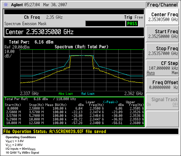
- +23dBm Transmit Power at 5% EVM and Meets Spectral Mask Requirements
- -79dBm Receive Sensitivity at 10% EVM
- 60dB of Transmit Gain-Control Range
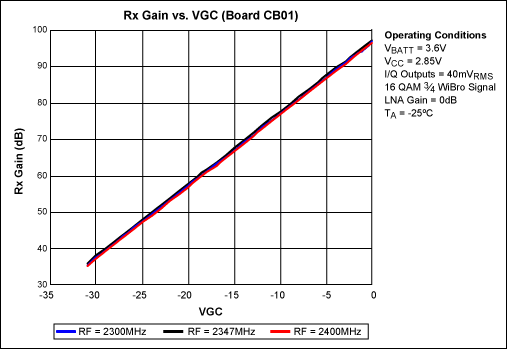
- 94dB of Receive Gain-Control Range
- Optimized Low-Current Modes

Lab Measurements
Supply Current Summary
VBATT = +3.6V, VCC = +2.85V, TA = +25°C
| Parameter | Test Conditions | Measured | Units |
| Shutdown Supply Current | MAX2837 and PA in shutdown; regulators and VCTCXO still active | 1.8 | mA |
| Idle Supply Current | MAX2837 in idle mode; PA in shutdown; regulators and VCTCXO active | 34.8 | mA |
| Transmit Supply Current | 16 QAM, ¾ FEC coding rate, POUT = +24dBm, EVM = 5% | 392.6 | mA |
| Receive Supply Current In | Low-current mode | 79 | mA |
| Receive Supply Current In | Nominal current mode | 96.2 | mA |
Receive Summary
VBATT = +3.6V, VCC = +2.85V, fRF = 2347MHz, VOUT = 90mVRMS, WiBro signal, RF specs are antenna referred, TA = +25°C
| Parameter | Test Conditions | Measured | Units | |
| DC Offset | I channels | 6.8 | mV | |
| Q channels | 4.5 | |||
| VGA Gain Step Size | 2 | dB | ||
| Receive Gain-Control Range | Max to min VGA gain | 61.7 | dB | |
| Receive LNA Gain Step | Attenuation from 0dB to -16dB | -15.9 | dB | |
| Attenuation from 0dB to -32dB | 32.1 | |||
| Gain Variation over Temperature | TA = -40°C to +85°C | LNA gain = 0dB | -5.2 | dB |
| LNA gain = -16dB | -5.3 | |||
| LNA gain = -32dB | -3 | |||
| Gain Variation over Frequency | fLO = 2304MHz to fLO = 2396MHz | 0.2 | dB | |
| Sensitivity at Low Supply Current¹ | 64 QAM, ¾ FEC coding rate, 10% EVM at sensitivity | -79.8 | dBm | |
| 16 QAM, ¾ FEC coding rate, 20% EVM at sensitivity | -90.7 | |||
| Sensitivity at Nominal Supply Current¹ | 64 QAM, ¾ FEC coding rate, 10% EVM at sensitivity | -80.4 | dBm | |
| 16 QAM, ¾ FEC coding rate, 20% EVM at sensitivity | -91.3 | |||
¹Rx EVM limits are at BB I/Q Rx outputs, and are given in the IEEE® 802.16e specification Table 338, "Receiver SNR Assumptions." The assumption is that this EVM for this modulation rate is sufficient to meet 1e-6 BER.
Transmit Summary
VBATT = +3.6V, VCC = +2.85V, fRF = 2347MHz, VIN = 90mVRMS, WiBro signal, RF specs are antenna referred, TA = +25°C
| Parameter | Test Conditions | Measured | Units |
| LO Leakage | Q = 640/352µA, I = 576/416µA | -39.6 | dBc |
| Sideband Suppression | I/Q phase = -0.5° | -52.5 | dBc |
| Transmit Power-Control Range | Including PA Gain Step | 64.5 | dB |
| Gain Variation over Frequency | fLO = 2304MHz to fLO = 2396MHz | 1.9 | dB |
| Transit EVM | 16 QAM, ¾ FEC coding rate, POUT = +24dBm, meeting spectral mask | 4.1 | % |
| Transit EVM | 16 QAM, ¾ FEC coding rate, POUT = +23dBm, meeting spectral mask | 3.5 | % |
Transit Operating Characteristics


Detailed Description
The WiBro reference design includes the following components: MAX2837 direct-conversion transceiver, Micro Mobio MMPA372X PA, MAX8510 regulators, Murata balanced-to-unbalanced SAW bandpass filters, Hexawave HWS466 SPDT Tx/Rx switch, and Vishay Si1563DH load switch.
The MAX2837 is a single-chip, wideband, direct-conversion transceiver designed for 2.3GHz to 2.7GHz WiBro and WiMax radios. The transceiver is fully equipped with an on-chip broadband VCO, fast settling sigma delta RF synthesizer, crystal oscillator, programmable lowpass filters, proprietary DC offset cancellation, I/Q error and carrier leakage detection circuits. The MAX2837 offers less than 1.4% of transmit EVM at -3dBm driver output power, and receive sensitivity better than -79dBm. When integrated with the MMPA372X PA and Murata BPF, the reference design can deliver at least 23dBm of output power at the antenna, while meeting WiBro EVM and spectral-mask requirements with margin


