要約
DS3902 is a response to market requirements for low cost solutions in Optical Modules which do not have stringent requirements for accurate temperature tracking of some laser characteristics; such as modulation current and extinction ratio.In addition, laser drivers having two closed loop control need a way of setting APC and modulation currents set points. Conventionally this has been done using mechanical potentiometers first, then these mechanical Pots are replaced with fixed resistors selected to have equal values.
Introduction
DS3902 is a response to market requirements for low-cost solutions in optical modules that do not have stringent requirements for accurate temperature tracking of some laser characteristics, such as modulation current and extinction ratio.
In addition, laser drivers that have two closed-loop controls need a way of setting APC and modulation currents set points. Conventionally this has been done using mechanical potentiometers first, then these mechanical pots are replaced with fixed resistors selected to have equal values.
This process relies on having fixed-value resistors to be close to the measured value of the pots. In practice, the fixed resistors do not match the pot values and the end result is that the optical-output power differs from the required settings. Therefore, it is introducing an error that translates into a larger optical-output power variation in the power budget.
Optical Module
Figure 1 depicts a typical low-cost optical module. The components comprising the module are:
- Optical Devices, Laser, and PD
- Laser /VCSEL Drivers
- TIA
- Limiting Amplifier
- DS3902
- Optional Serial EEPROM
- Power Management and Surge Control
The EEPROM could be used for serial ID information required in some modules. The module footprint could be either SFF or SFP compliant.

Figure 1. Typical optical module block diagram.
DS3902 and Serial EEPROM
The two variable resistors in DS3902 are used to set bias and modulation currents. The settings are done through I2C interface. Some modules may require additional EEPROM. This is typically used for serial ID information, and new modules may need to include this feature. DS3902 has programmable address, therefore connecting it to a single I2C bus line (with other devices) without any additional components.
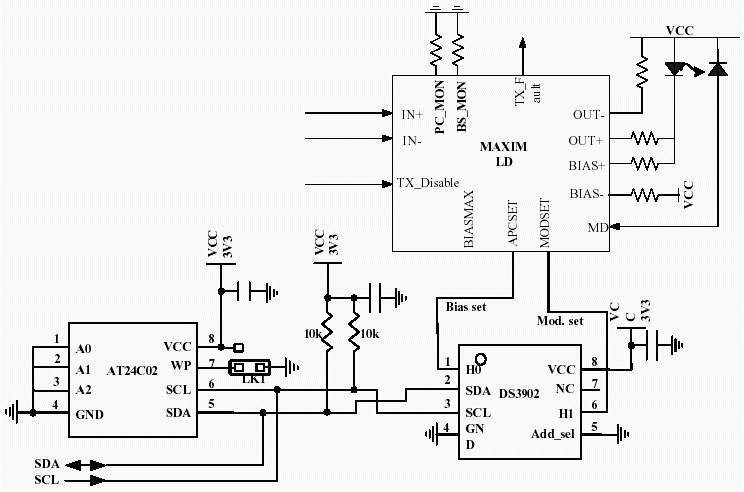
Figure 2 shows connection details for using DS3902 and a serial EEPROM (ATmel AT24C02) on a common I2C interface. Also Figure 2 illustrates connections to a laser driver.

Figure 2. Schematic for LD, DS3902, and AT24C02.
The DS3902's default address is A2h (Add_sel = 0). If an address different from A2h is required, Add_sel will be pulled high. Register 00h content is the device address when Add_sel = 1. In the above schematic AT24C02 is configured for A0h address, (A0 = A1 = A2 = 0).
The WP (write-protect) pin connects to ground using a link, allowing R/W access to memory locations. Once the memory is programmed, the WP pin can be pulled high through LK1, to prevent accidental write. DS3902 has S/W protection scheme, whereby access to memory is only possible with password.
The choice of laser driver depends on the specific application and there are a number of Analog Devices laser drivers to choose from.
ROSA and TOSA
RX Optical Sub-Assembly (ROSA) and TOSA's are normally required at higher bit rate systems. At lower bit rates, less than or equal to 2.5Gbps, driver ICs are used close to the laser and achieve good performance. Conversely, ROSAs (PIN TIAs) are required for bit rates above 622Mbps in order to achieve reasonable sensitivities.
Laser drivers incorporate a number of features including:
- Average Power Control (APC)
- Extinction Ratio (ER) Control is Implemented in Some Laser Drivers
- Laser Safety Functions
- TX_Disable Function
- TX_Fault Function
Some laser drivers incorporate pulse-width control of the incoming signal stream as well as clock input for better jitter performance.
Limiting Amplifier
Signal amplification following the TIA is achieved using a limiting amplifier. This is typically a high-gain stage in order to provide a reasonable constant amplitude (>200mV) to the host board. It also has to be able to drive low impedance transmission lines.
In addition, loss-of-signal detection is done typically in the limiting amplifier stage and flagged to the host board with a logic-high level. Threshold and sampling time adjustment may also be incorporated in this stage.
Power Management and Surge Control
In order to allow hot plugging into the host board, SFF MSA for GBICs requires surge control of the module's power supply. This is normally 10% of the nominal current consumption. For GBIC it is 30mA. Also, depending on the detail design and the individual ICs used some sequencing may be required. Timing requirements normally impose specific slow-start timing.
A typical slow-start circuit is depicted here. This is a low-cost design with minimum of component counts.

Figure 3. Schematic diagram for low-cost, slow-start, power supply design.
All components are SMD and available in small footprints. M1 is a PMOS and should be selected for adequate current ratings and minimum voltage drops across it when supplying full current. Component values could be adjusted if needs be. The values given here provide a practical slow-start timing.
The following diagram for RL = 9Ω is a 360mA load, and timing delay is given for three values of C3.

The above is response to a step-input voltage 0V to 3.3V. The current surge is well below the 360mA maximum current output with the component values given in the schematic.


