µPower Precision Dual Op Amp Combines the Advantages of Bipolar and CMOS Amplifiers
µPower Precision Dual Op Amp Combines the Advantages of Bipolar and CMOS Amplifiers
2005年09月01日
Introduction
The LTC6078 and LTC6079 are dual and quad micropower, precision op amps that combine the low offset and drift of traditional bipolar amplifiers with the low bias current of CMOS amplifiers. Additionally, the LTC6078 features low supply current and low noise, low supply voltage operation, and rail-to-rail input and output stages. This combination of features allows precision performance previously available only through composite amplifiers, manual offset trimming, or calibration.
A Superior Op Amp
Traditional bipolar op amps can be designed for excellent precision over temperature, but bipolar amplifiers lack the low bias currents of CMOS amplifiers. In high source impedance applications, a few nanoamps of input bias current can equal millivolts or more of input error, swamping the amplifier’s low VOS.
Traditional (and some non-traditional) CMOS amplifiers come with their own set of strengths and weaknesses. Input bias current can be much lower than their bipolar counterparts. But VOS and VOS drift specifications often limit the usefulness of these amplifiers in high-precision applications, presenting the opposite problem of bipolar amplifiers. Chopper-stabilized (also known as zero drift) amplifiers, which are generally CMOS based, employ a synchronous offset cancellation scheme to negate the DC imperfections of the amplifier, so that VOS and VOS drift of the amplifier become almost negligible. However, zero drift amplifiers tend to draw much more current than their continuous-time counterparts, precluding their use in low-power precision applications. Additionally, zero drift amplifiers may be much noisier at higher frequencies due to auto-zero circuit clock harmonics.
The LTC6078 is a CMOS op amp with a proprietary VOS trimming circuit that yields 25µV maximum VOS and 0.7µV/°C maximum VOS drift, lowest among all comparable bipolar and CMOS op amps. Combined with the 50pA maximum input bias current over the entire temperature range, the LTC6078 is ideal for all precision or high-impedance instrumentation applications. The low 54µA supply current and 2.7V minimum supply voltage make the LTC6078 an excellent choice for power-sensitive or hermetically sealed circuits. An LTC6078 dual op amp circuit with passive high-impedance sensors can run on two alkaline AA batteries for over 1.5 years.
Precision Current Sense and Control
The LTC6078’s rail-to-rail input and output stages allow precision input sensing right at VDD or VSS, which is useful for simple high-side or low-side current sensing. Figure 1 shows the LTC6078 in a simple, precise high-side current sensing application. The 25µV precision translates to excellent current resolution with a very small sense resistor, meaning more precision with less power loss. Used in a feedback loop, the LTC6078 can be used as a precision current source/sink or as a current servo.
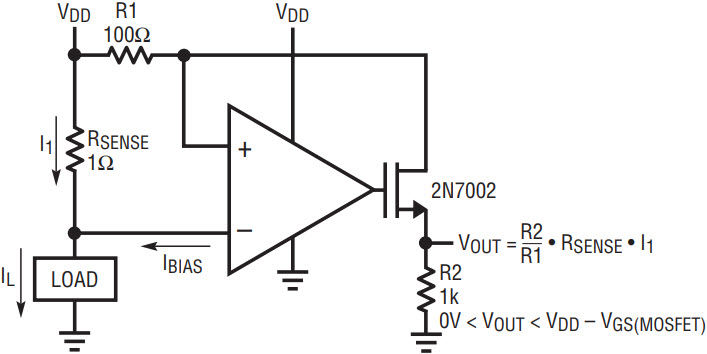
Figure 1. Precision, low-supply-voltage current sense amplifier. The LTC6078 servos the N-channel MOSFET drain current so that the voltage across R1 is the same as the voltage across the sense resistor. The precision of the LTC6078 enables a small sense resistor to be used for less power dissipation without sacrificing DC accuracy.
Figure 2 shows the LTC6078 balancing the loads on two paralleled LT1763 low dropout (LDO) voltage regulators. A common practice when paralleling two voltage regulators is to simply tie the two outputs together. However, internal voltage offsets cause one regulator to handle the bulk (or all) of the load current. In the case of sink-source regulators, one may be sourcing a great deal of current into the other regulator!
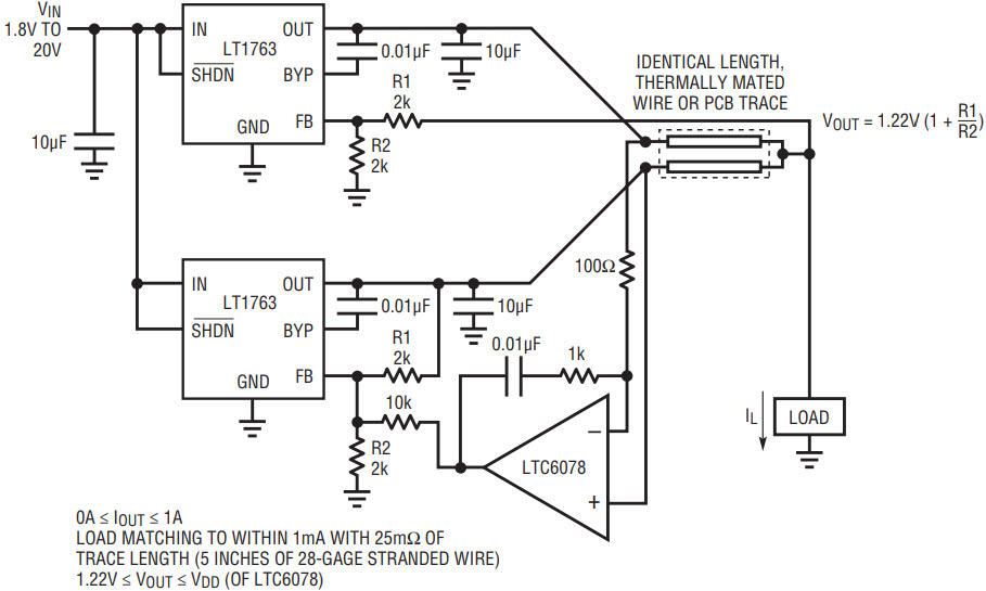
Figure 2. The LTC6078 used as a current load balancing servo amplifier. Short lengths of copper wire or PCB trace can be used as ballast resistors due to the LTC6078’s precision. VDD of the LTC6078 may be connected to VIN or VOUT, as long as the minimum 2.7V supply voltage requirement is met.
Load sharing circuits work best when the contribution to output current is balanced between the regulators. The LTC6078 compares the voltage outputs of the two LDOs and servos the feedback pin of the second to balance them. The high precision of the LTC6078 means that discrete ballast resistors are unnecessary—short pieces of wire or PCB trace are sufficient to provide the ballast resistance. With 25mΩ of resistance1, the LTC6078 can balance the current sharing of the LDOs to be within 1mA, regardless of the absolute load current output. The feedback network does not noticeably degrade the load transient performance of the regulators, and Figure 2 can be expanded to include as many paralleled regulators as necessary.
Shutdown Function
For extremely low power applications such as hermetically sealed battery-powered sensors, the 10-pin version of the LTC6078 in the tiny DFN package offers two shutdown pins (one for each amplifier). When in shutdown mode, the low 54µA per amplifier current draw is reduced to a maximum of 1µA (over the entire temperature range). The fast 50µs turn-on and 2µs turnoff times ensure that minimal power is dissipated during the transition periods.
In applications where many inputs need to be monitored and only a single analog-to-digital converter is available, the independent shutdown function of the two amplifiers allows any number of LTC6078 outputs to be multiplexed together. The high-impedance output of the LTC6078 in shutdown mode does not load the output of an active LTC6078. So long as two amplifiers are not simultaneously active, there is no need for external multiplexing components.
Layout Considerations
In high source impedance applications such as pH probes, photodiodes, strain gauges, et cetera, the LTC6078’s low input bias current (50pA maximum over temperature) requires a clean board layout to minimize additional leakage current into a high-impedance signal node. A mere 100GΩ of PC board resistance between a 5V supply trace and an input trace adds 50pA of leakage current, which is typically greater than the input bias current of the LTC6078. For comparison, a bit of unwashed soldering flux can add a 1GΩ–10GΩ resistance. In critical applications, or if leakage is suspected, a guard ring around the high-impedance input traces driven by a low-impedance source to equal the input voltage prevents such leakage problems. The guard ring should extend as far as necessary to shield the high-impedance signal from any and all potential leakage paths. Figure 3 shows the recommended layout when using a guard ring.
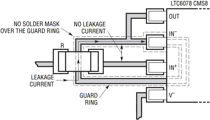
Figure 3. A sample layout using a low-impedance guard ring to shield a high-impedance signal trace from board leakage sources. The output pin can drive the guard ring directly or through a low impedance (<100kΩ) feedback resistor. The amplifier is shown in a non-inverting gain configuration.
Conclusion
The LTC6078 offers all of the benefits of both bipolar and CMOS amplifiers, as well as a slew of other features that make it the ultimate choice for low power, precision applications. The combination of excellent offset, drift, and input bias current specifications is unmatched among both bipolar and CMOS op amp offerings. For applications requiring four precision op amps, the LTC6079 is available in 16-pin surface-mount SSOP and DFN packages.
Notes:
1 A 25mΩ resistor is equal to approximately 5 inches of AWG 28 gauge copper stranded wire or 1.25 inches of a 25 mil wide one-ounce copper PCB trace at room temperature.


